


To improve the reliable integration of additively manufactured (AM) metal components, there is an urgent need for surface finishing methods capable of processing rough, “as-printed” surfaces.
 Timothy J. Gorey, Jamie A. Stull, Robert E. Hackenberg, Courtney L. Clark, and Daniel E. Hooks.We present a new and scalable electropolishing (EP) technique for use on AM 316L stainless steel (SS) that is capable of achieving a surface roughness equivalent to a machined finish, with arithmetic mean heights (Sa) as low as 1.0 µm. This technique utilizes the sequential application of a new, NaCl/H2O pulse/pulse reverse (P/PR) EP step along with a conventional DC (direct current) EP step, where P/PR expands the capability of EP by removing roughness features > 1 µm, which has been previously unattainable with DC EP alone without substantial material removal. This is achieved by independently varying pulse parameters, such as pulse width and height, allowing more control over electrodynamic processes at the part-electrolyte interface.
Additionally, P/PR EP resulted in higher smoothing efficiency, where a higher degree of smoothing was achieved with less material removal when compared with conventional DC EP alone. This minimizes unwanted change in geometry from excessive metal dissolution.
Introduction
State of the Field—Addressing Roughness on Additive Surfaces
The quality of additively manufactured (AM) metal parts has significantly improved since the advent of the technology, and its application is already positively impacting a range of industries.1,2,3 316L stainless steel (SS) is an appealing material for AM due to its high corrosion resistance and strength.4,5,6 However, the manufacturing capabilities for AM 316L SS is currently outpacing post-processing techniques, as the parts suffer from high surface roughness resulting from the printing process.2,7,8,9,10,11,12 It is typical for these samples to have arithmetical mean height distributions (Sa) in the order of 5–15 µm, which is problematic since many surface finishing techniques, such as coatings, and production applications require a surface roughness around 1 µm or less.9,13,14,15 Inferior part tolerance and corrosion resistance originating from surface roughness are currently preventing practical integration of AM parts. Previously, studies have reported a higher corrosion susceptibility for AM 316L SS as compared to traditionally machined metal surfaces, and it is postulated that active site defects related to surface roughness is a contributing factor.16
Mechanical polishing, tumble polishing, and electropolishing have historically been used, singularly or in sequence for standard surface finishing of machined parts in an attempt to alleviate roughness related problems.12,17,18,19,20 Though mechanical and tumble polishing can achieve acceptable finishes for different applications, achieving homogeneous roughness across every surface of complex, single-component parts is still a challenge.12,21 Instead, electropolishing (EP) is the most appealing approach for AM metals, due to full part submersion allowing for internal surfaces in contact with the electrolyte to be polished.21 Direct current (DC) EP has been an industry standard for decades and employs concentrated acid electrolytes, such as sulfuric and phosphoric acids. Jacquet and Elmore provided the earliest explanations of DC EP, which is an electrolytic process that reduces the surface roughness of metal parts and typically results in a bright, smooth finish.22,23,24 Jacquet attributed the reduction of surface roughness to the formation of a viscous ionic layer at the surface of the anode, proposing that non-uniform thickness of this layer results in ohmic variation between the electrodes and surface asperities (i.e., surface protrusions contributing to roughness are closer to the counter electrode).25 Thus, the formed gradient in solution resistance leads to the preferential dissolution of those protrusions on the part surface. DC EP has been applied to a range of AM metals, though these processes were unable to adequately reduce roughness of the initially very rough parts to within the engineering requirements for the given application.12,21,26,27,28 For this reason, pulsed EP processes are being examined.
The field of pulse/pulse reverse (P/PR) EP is still relatively novel, with theory and specific processes still being gradually elucidated.18,29 Recently, the method has been popularized by Faraday Technology, Inc., which has been vital in advancing the field. Faraday has put forward multiple publications and patents aiming to establish guiding principles on the implementation of pulsed EP processes for various non-AM metals.30,31,32,33,34,35,36,37 The incorporation of a reverse pulse (cathodic pulse) has shown great promise in further advancement of the technique by granting increased process control through tuning and optimization of waveform parameters, as well as other environmental variables (temperature, agitation). Cathodic pulsing periodically reduces/depassivates oxide build-up, thus mitigating the need for complex and environmentally harmful chemical additives that have historically served this purpose.23,24,29,30,31,35,38,39,40,41
For example, Zhou et al. patented a process for electrochemical machining through the application of modulated reverse electric fields in aqueous sodium chloride and sodium nitrate (NaCl/NaNO3) solution.35Additionally, Taylor et al. proposed using a 12% (w/w) aqueous NaCl solution to EP 1010 steel coupons; this resulted in the development of a commercially relevant processing method in the auto industry.42 While the P/PR EP method has been applied to a range of traditionally manufactured (i.e., wrought or machined) metals, including SS and passive materials, such as titanium and niobium, application to AM metals is unexplored. The elevated level of process control with P/PR EP has garnered interest in its application to AM due to traditional DC EP being unable to adequately smooth these surfaces.
Pulse/Pulse Reverse Electropolishing—Description of Parameters
Selecting electrolyte and pulse parameters can be challenging when applying P/PR EP to AM SS, due to the high dimensionality of pulsed methods (i.e., there are many combinations of the pulse and electrolyte parameters). Regarding electrolyte parameters, Table I lists important conditions that must be considered when designing a pulse sequence. These parameters are often “upstream” of the pulse parameters, as the electrodynamic processes are typically a function of the electrolyte conditions. For example, current and voltage will depend on the concentration and conductivity of the electrolyte. It is thus useful to have electrolyte conditions selected before choosing pulse parameters.
Table I Electrolyte parameters and definitions
| Parameter | Definition |
| D | Diffusivity of electrochemically active species |
| Cb | Bulk concentration of electrochemically active species |
| T | Electrolyte temperature |
| S | Conductivity of the electrolyte |
| U | Electrolyte velocity (agitation rate) |
| X | Electrolyte species |
These parameters can be tuned and must be considered when designing a pulse sequence.
Regarding pulse parameters, determining effective current (charge transfer per time) and integrated effective current (total charge transfer from EP) is necessary for sample-to-sample comparison and predicting the amount of material removed. Figure 1 shows the generic anatomy of a pulse sequence used for P/PR EP and the parameters necessary for calculating the effective and integrated effective currents. Note that the sequence is plotted versus voltage. This can be readily interchanged with current, where peak anodic and cathodic voltage (Vpeak,anodic and Vpeak,cathodic) can also be referred to as the analogous peak currents, Ipeak,anodic and Ipeak,cathodic. Equations 1–3 show how equivalent DC current in P/PR (ieff) is calculated for comparison with DC EP samples. First, the duty cycles in the anodic and cathodic directions must be individually calculated by accounting for the fractional amount of time current is actively flowing over the course of both on time (ton) and off time (toff) in the anodic and cathodic directions [shown in Eqs. 1–2].
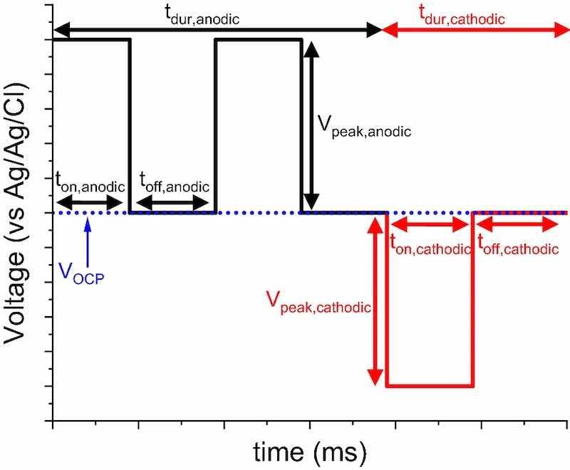
Fig. 1: The anatomy of a pulse sequence used for P/PR EP. The pulse parameters are labeled and can be used to control electrodynamic aspects. ton values correspond to when current is actively flowing, whereas toff is when no current is flowing. tdur is the duration of either the anodic or cathodic sequence. Vpeak values are the peak height, and VOCP is the open circuit potential.
Note that the number of pulses in each anodic or cathodic part of the sequence (manodic and mcathodic) must be included in the numerators. To demonstrate with Fig. 1 as an example, if ton,anodic, ton,cathodic, toff,anodic, and toff,cathodic all equal 2 ms, then tduty,anodic = (2·2)/(8 + 4) and tduty,cathodic = (1·2)/(8 + 4). Next, Eq. 3 shows how the net effective current density (ieff) is calculated by accounting for current in the anodic and cathodic directions. For this study, peak current in the anodic direction is negative.
(3)
Finally, Eq. 4 demonstrates how the integrated current density (iint,eff) (i.e., the total amount of charge transfer) can be calculated over the entire P/PR EP process by multiplying ieff by the total amount of time the part is exposed to the pulse sequence, tEP.
(4)
Using the above equations to determine ieff, iint,eff can be held constant by varying tEP experimentally; this allows direct sample-to-sample comparison, even if samples are subjected to different pulse sequences. In short, each sample can undergo the same amount of material removal, independent of the pulse parameters chosen.
Pulse Parameter Selection
For selecting pulse parameters, Taylor et al. and Hall et al. have published general guidance, and understanding the theory behind P/PR EP is important to designing an effective waveform.30,32,42 Additionally, Inman et al. discussed P/PR waveform sequencing for EP following a series of experiments where the primary (ohmic-limited current), secondary (electron transfer-limited), and tertiary (diffusion-limited) current distributions, as well as different boundary conditions and processing parameters were varied.43 Knowing the type of current distribution, either primary/secondary or tertiary is important for targeting the correct surface features. To determine and control the type of current distribution, a transition time, τ, can be calculated, which approximates the amount of time needed to consume all electrochemically active species at the electrolyte-part interface.42 Once the full surface concentration of species is consumed, diffusion of material from the bulk becomes necessary to sustain the electrolytic reaction. This is the point where the current distribution transitions from primary/secondary towards tertiary current distribution. Equation 5, which was originally proposed by Taylor et al., shows how τ can be calculated using ipeak,anodic and bulk solution concentration, Cb:
(5)
where n is the electron exchange stoichiometry, F is Faraday’s constant and D is the electrochemically active species diffusivity.42 The primary factors controlling τ are thus Cb and ipeak,anodic, each with square dependences. In knowing τ, ton,anodic can be tuned towards either primary/secondary or tertiary current distribution by setting ton,anodic to be smaller or larger than τ, respectively. Choosing a type of current distribution will ultimately control the size of asperity removed. Figure 2 provides guidance on the relationship between qualitative surface finish and pulse parameter selection. Macro-smoothing is the most relevant for processing AM metals, where large-scale waviness persists after traditional DC EP. Macro-smoothing, i.e., smoothing asperities > 1 µm can be accomplished with short, intense pulses and a small diffusion layer, such that primary/secondary current distribution dominates.36,42 To design a pulse sequence for macro-smoothing, ton,anodic should be chosen to be shorter than τ for a given Cb and ipeak,anodic.
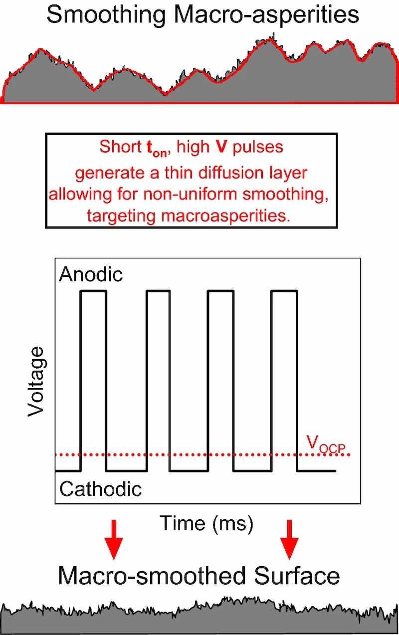
Fig. 2: Method used for selecting pulse parameters to smooth macro-asperities. The top schematic is the part surface before macro-smoothing, and the bottom is the expected surface finish of a macro-smoothed part. VOCP is the open circuit potential, i.e., the potential where no current flows.
Selection of toff,anodic and toff,cathodic are less crucial; simply, toff should be sufficiently long to eliminate any diffusion effects caused by either the consumption of acceptor ion species or the build-up of dissolved metal ions at the sample-solution interface. Diffusion distance, x, with no electric field applied can be estimated as:
(6)
where D is the diffusivity of the acceptor ions. For example, Cl- and OH- at 0°C have x ≈ 1.2 and 3.2 µm, respectively, when toff = 1 ms. In macro-smoothing, where ton values are below τ, and the diffusion distance is ~ 104 times thicker than the surface layer of ions, it is reasonable to assume all electrochemically active species at the interface will be replenished to bulk concentration by the end of each toff period.42
The toff parameter has additional advantages. In DC EP, electrolyte temperature can become a limiting factor for large surface area parts requiring high current. For example, high power systems often require recirculation chillers, as high temperatures can degrade the quality of the finish. In P/PR EP, toff can be extended to allow heat to dissipate in between pulses. Provided toff is sufficiently large to eliminate diffusional effects, extending toff has no effect on surface finish, other than those induced by the changes in electrolyte temperature.
Experimental Goals
In this study, we present a post-processing method for AM 316L SS using P/PR EP techniques. Additionally, a series of experiments is shown to demonstrate how pulse parameters can be selected, optimized, and compared with alternative EP methods, such as DC EP. We will show that the combination of P/PR and DC EP methods yields a remarkably smooth surface for AM parts, as well as a method for estimating material removal. These greener alternatives offer a promising future for the surface finishing industry that both expands the smoothing capability of EP to challenging surfaces, such as AM 316L SS, and offers a promising replacement or augmentation to traditional DC EP methods.
Experimental
Additively Manufactured 316L Stainless Steel Samples
316L SS powder (Carpenter Additive) was rendered under argon by direct metal laser sintering using an EOS M290 into parallelogram-shaped samples at 928.1 mm/s and a laser power of 214.2 W. Sample porosity ranged between 0.01 and 0.02%, with a density of 7.8429 g/cm3. Due to the small, simple geometry of the parallelogram test objects, no support structures were used, though it should be noted that support structures might leave deep, difficult-to-remove defects, and removal of such defects was not explored in this study. This parallelogram shape was chosen because it offers a variety of surface orientations, or “skins,” each with different Sa properties; these are shown in Fig. 3. While future studies will examine other surfaces, side-skin surfaces were the focus for this study. Parallelogram samples were cut in half long-ways (bisecting line #1 in Fig. 3), which generates two coupons with side-skin faces. Prior to measurement and EP, each coupon underwent sonication in isopropanol followed by sonication in deionized water; however, the coupons did not undergo strain relief/heat treatment after printing. Thus, some residual strain is expected but was not measured. Previous work has shown that strain relief can be imparted by surface treatment, though this relief is derived from material properties (e.g., porosity, microstructure) which are controlled by the print parameters.44
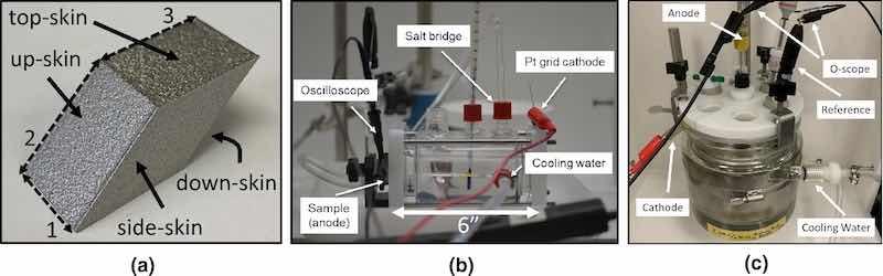
Fig. 3: (a) As-printed AM 316L SS parallelogram sample dimensions and skin orientations. Line lengths for each line are (1) 13.0 mm, (2) 18.0 mm, and (3) 18.0 mm. (b) Photograph of the BioLogic flat cell with connections and anode–cathode distance. (c) Photograph of up-scaled Pine Research Reactor for EP of full parallelograms. Cell is 14 cm tall with diameter = 11.4 cm. Anode–cathode distance ≈ 5 cm.
Electropolishing Methods
EP studies were performed in a BioLogic flat cell reactor, shown in Fig. 3b, which allows the anode–cathode distance to be consistently set at 6″ (15.2 cm). O-rings (1 cm2) were fixed to the side-skin surface of each coupon using Devcon 5-min epoxy, and coupons were clamped to a 1-cm2 orifice on the flat cell with the coupon surface normal to the bench top. For P/PR EP, the cell was filled with 200 ml of aqueous 2.6 M NaCl (Sigma Aldrich) electrolyte. For DC EP, 200 ml of EPS 2500 commercial electrolyte (H2SO4, H3PO4, and proprietary additives) was used. The cell is equipped with a cooling/heating water jacket and thermometer port for electrolyte temperature control, and a salt bridge for the reference electrode, where a Ag/AgCl electrode was used for reference measurements. A 5 × 5 cm platinized titanium grid (surface area >> 1.0 cm2) was used as the counter electrode and installed 6″ from the coupon surface (i.e., 15.2 cm of electrolyte between the coupon and counter electrode), also normal to the benchtop and parallel to the coupon surface. EP was performed using a Dynatronix DPR20-30-100XR pulse power supply and monitored using a Tektronix TBS 2000 oscilloscope. Reported current densities and effective DC currents (equivalents) were calculated using equations in the Dynatronix manual; these equations are explained above to provide guidance on pulse parameter selection. Though agitation will certainly have an effect, to isolate other variables there was no agitation in these experiments.
A full parallelogram test object was separately electropolished in a 1-l jacketed “OpenTop” Pine Research cell. The cell was cylindrical in shape, and a SS counter electrode conformally lined the inside of the cell, forming a cylindrical shape. Parallelograms were spot-welded to a SS wire and centered in the cylindrical counter electrode with stop-off compound applied to the wire, where it contacted the electrolyte. The average distance between the closest edges of the part and cylindrical counter electrode were ~ 5 cm. For all EP experiments (both DC and P/PR), samples were immediately and thoroughly rinsed in DI water to remove any residual electrolyte, which is a method recommended by the commercial EPS 2500 electrolyte manufacturer.
Roughness and Imaging Methods
Surface roughness measurements were performed using a Zygo ZeGage Plus 3D profilometer. For consistency, each coupon was leveled perpendicular to the Zygo light source prior to measurement. Because AM 316L SS can have slightly spatially dependent roughness properties, even within the same part, a minimum area of 1.5 × 1.5 mm was measured for each coupon with the Sa being reported as a metric for roughness. As shown in Fig. 4, each measurement generates a 3D topographical map, and 2D slice images can be drawn across the 3D map to extract profile line scans. It is important that this is done consistently, as AM components can have some periodicity in roughness, such as print lines. Thus, all line scans across these features were drawn in the same direction for accurate comparison. Note, that Sa was generated from 3D images, whereas Ra was used for line scans. Because Sa is a better statistical representation for roughness, that value is reported, even on the line scan graphs below. For qualitative comparison, scanning electron microscopy (SEM) images were collected using an FEI Inspect, and optical photographs were taken using a Nikon D610 camera with macro lens.
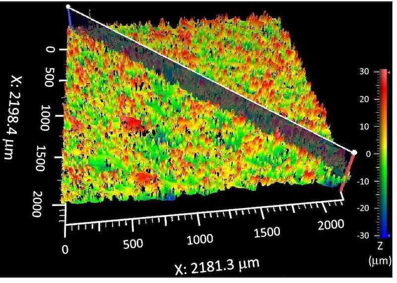
Fig. 4: Representative 3D image taken by Zygo ZeGage of as-printed side skin surface. 2D slides are taken diagonally (shown) with all samples leveled and in the same orientation.
Results and Discussion
Results are presented in the following Sections. First, traditional DC EP is performed on a coupon to represent the current industrial capability and establish a basis for comparison. Second, a method for selecting P/PR EP parameters is discussed, and P/PR EP coupons are compared with that processed by DC EP. Then, P/PR and DC EP are combined and compared with the preceding coupons. Last, a method for P/PR EP is introduced that explains how surface finish can be optimized while minimizing the amount of dissolved material.
DC Electropolishing
To provide a reference for comparing P/PR EP methods, a coupon was DC electropolished using commercial electrolyte EPS 2500 (Electro Polish Systems). In the BioLogic jacketed reactor, 250 ml of EPS 2500 was heated to 90°C, and the defined 1-cm2 coupon surface was electropolished at ieff = − 0.281 A/cm2 up to a total ieff,int = − 15 A * min/cm2 (these parameters are recommended by manufacturer). Profilometry and mass was measured before and after EP to quantify changes in Sa and mass (ΔM). Geometry change was approximated and plotted with the line scan profilometry data to approximate change in height relative to the roughness. Density was measured by printing duplicate shapes of known volume and measuring the mass. Using this density (7.8429 g/cm3) and ΔM due to EP within the defined 1 cm2 o-ring area, A, the volume of dissolved metal, Vdissolved can be calculated:
(7)
If a cylindrical volume is assumed, i.e., the 1 cm2 o-ring constrains lateral etching, the distance dissolved into the surface, h, can be approximated as
(8)
Figure 5 shows AM 316L SS coupon photos, micrographs, and profilometry data (a) before and (b) after DC EP. The micrographs of the as-printed material show a variety of roughness type, with large, macro-scale fused particles (diameter = tens of microns) and small, micro-scale roughness, such as small ridges in between the particles, in the single micron and smaller regime. This bifurcation of roughness type will be generally termed macro- and micro- roughness, where “micro-” refers to asperities < 1 µm and “macro-” refers to the fused particles or waviness of the coupon surface visible to the naked eye, i.e., the coupon photographs. Note that the fused particles seen in the micrographs are not identifiable in the profilometry measurement. This is due to missing data points around the base of the fused particle, which are automatically filled in by the graphing software. While this shadowing effect is not expected to significantly change the Sa values, it will influence the line shape of the profilometry scans. For the DC EP coupon, there is a bright, mirror-like finish, indicating the removal of roughness at the scale of the wavelength of light, where light would otherwise have been scattered in different directions. Fused particles are also removed. However, macro features, such as waviness, are identifiable in the optical pictures, micrographs, and profilometry results even after DC EP. Thus, this method is only effective at removing micro-asperities for AM 316L SS. Regarding quantified roughness, the Sa was reduced from 9.0 µm to 3.1 µm, with a mass loss of 0.062 g from the 1-cm2 region. This ΔM resulted in a considerable 80.3 µm loss in material Z height, which is reflected as an offset in the EP profilometry line scan leading to concerns with maintaining part tolerances. In summary, DC EP can be used to remove large, fused particles and reduce Sa for AM 316L SS, though considerable mass loss and geometry change is necessary to obtain such improvements.
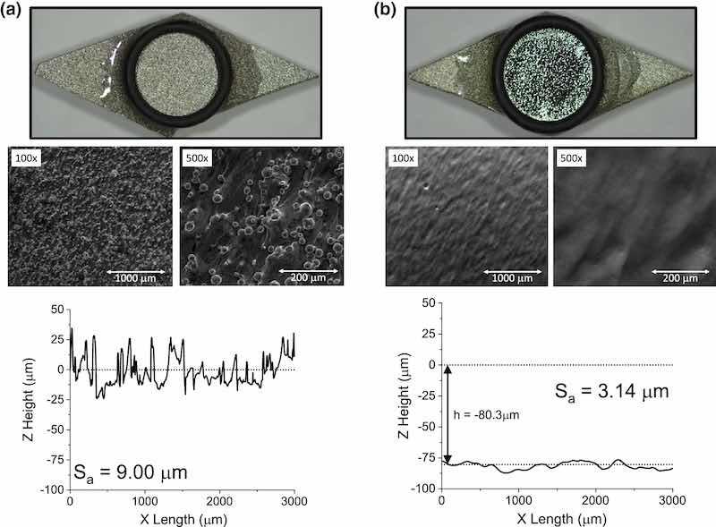
Fig. 5: (a) Photographic and SEM images of as-printed 316L SS coupons are shown along with line scan profilometry data (bottom). (b) Analogous results for a coupon after DC EP. Dotted lines in the profilometry scan represent the average Z height. Note: Sa values are from area scans, not line scans.
The mechanism by which DC EP preferentially removes roughness is well understood and originates from a combination of primary (conductivity-controlled) and tertiary (diffusion-controlled) current distribution. The onset of the DC field creates a depletion layer, where acceptor ion species are consumed and replaced with less conductive metal ions dissolving into solution at the part surface. This forms a concentration gradient at the near surface, growing in thickness until a steady state is reached, where reaction kinetics are in equilibrium with diffusion kinetics. This diffusion layer thickness is relevant in the context of the asperity size, where a micro-profile exists when the diffusion layer thickness is equal to or smaller than the asperity size and results in preferential removal of peaks relative to the recesses.32,40,45 Thus, in DC EP, the electric field is focused on asperities due to formation of the resistive diffusion layer, which increases the voltage gradient between the peaks and recesses.23,24 The final, mirror-like finish suggests that many of these asperity sizes are in the order of the wavelength of light.
Pulse/Pulse Reverse Electropolishing Parameter Selection
As discussed above, P/PR EP is a promising alternative or augmentation to DC EP, particularly for AM metals, because macro-level waviness can be targeted via electrodynamic processes by independently varying each pulse parameter. The challenge of high dimensionality makes it necessary to conduct fundamental experiments that explore the relationships between parameters, such as ton,anodic and surface finish/Sa. The following experiment is an example of this, where pulse widths (ton,anodic and ton,cathodic) were varied, with all other pulse and electrolyte parameters held constant. Other pulse and electrolyte parameters have been explored as well, but they are not reported here. In this example, a 2.6-M NaCl/H2O electrolyte at 2.5°C was used to ensure a consistent conductivity. For simplicity, anodic and cathodic pulse widths were always selected to have the same pulse height and width, i.e., ipeak,anodic = ipeak,cathodic and ton,anodic = ton,cathodic. For comparison with the DC EP coupon, ieff for the P/PR EP coupon was held constant, which was − 0.281 A/cm2. Using Eqs. 1–3, ipeak,anodic and ipeak,cathodic were calculated at each ton value, yielding ± 0.936 A/cm2 for both coupons. When varying ton,anodic and ton,cathodic, it is important to maintain constant Iint,eff, such that each coupon undergoes the same amount of charge transfer per cm2. For this pulse sequence, a 4:1 anodic:cathodic pulse ratio was selected; it is thus expected, per Eqs. 1–3, that ieff will become more anodic with increasing ton,anodic. Therefore, to keep int,eff constant between coupons, Eq. 4 was used to calculate EP duration (tEP), such that each received − 7.5 A*min/cm2 of charge. This value represents half of the charge received by the prior DC EP coupon; this was done for purposes explained below. Note that because ipeak,anodic and Cb (NaCl/H2O) are constant across all coupons, τ will also be constant; using Eq. 5, τ ≈ 1500 ms.
A series of on times (ton,anodic and ton,cathodic) less than τ were selected for a set of coupons to optimize reduction of macro-scale roughness ton,anodic = ton,cathodic = 0.2 ms, 1 ms, 5 ms, 25 ms, 125 ms, and 625 ms pulse widths were chosen; additionally, toff,anodic = toff,cathodic = 1 ms for all coupons. As discussed with Eq. 6, 1 ms will be sufficiently long to allow replenishment of bulk surface concentrations of the electrochemically active species (i.e., Cl- and OH-) and the diffusion of metal ions away from the coupon surface in between pulses. As with the DC EP coupon, change in Sa and mass were measured for each coupon before and after P/PR EP. Due to slight variation in initial roughness of the as-printed coupons, Sa values obtained from these measurements were used to calculate percent change in Sa.
Figure 6 shows the percent change in surface roughness with increasing pulse width after P/PR EP; absolute Sa values for each coupon can be found in Table II. Generally, there is an inverse correlation between % change in Sa and ton, with the largest improvement being obtained at short pulse widths and the least improvement being obtained with longer pulses. In principle, there should be no difference in roughness for any of these coupons, since the ton values are below diffusion-influenced dynamics. However, since there is no agitation in the cell this is not the case. As ton increases under these conditions, the off times required to allow dissolved species to diffuse away occur less frequently and lead to the accumulation of byproducts at the part-solution interface during the on pulse. Coupons with pulse widths greater than 5 ms began to show surface streaking due to the accumulation of gas on the surface, becoming more severe as ton,cathodicincreased. By ton = 25 ms, surface pitting becomes noticeable around the o-ring edges, where diffusion is poor. By ton = 625 ms, considerable oxidation/uncontrolled corrosion of the SS is observed (indicated by discoloration of the surface), likely due to H+ and OH− build-up at the surface before being cathodically depassivated or having time to diffuse away during toff. Pitting of the surface of the coupon at ton = 625 ms was accompanied by an increase in Sa, above that of the as-printed value. There was no coupon-to-coupon variation in ΔM, with each losing 12.0 mg of material; this is expected due to each coupon receiving iint,eff = − 7.5 A*min/cm2.
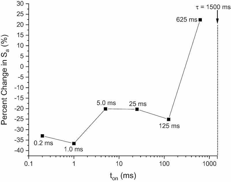
Fig. 6: Percent change in surface roughness is plotted as a function of increasing pulse width (where ton = ton,anodic = ton,cathodic for each coupon). Pulse width was increased by a factor of 5 for each separate coupon. All times were kept below transition time (τ) to eliminate diffusion-limited reactions.
Table II Absolute Sa values for coupons in the P/PR EP ton study
| ton;anodic = ton;cathodic (ms) | Initial Sa (µm) | Final Sa (µm) | % Change |
| 0.2 | 9.52 | 6.38 | − 33 |
| 1.0 | 8.68 | 5.50 | − 37 |
| 5.0 | 8.69 | 6.94 | − 20 |
| 25 | 7.54 | 6.01 | − 20 |
| 125 | 7.33 | 5.49 | − 25 |
| 625 | 7.22 | 8.84 | + 22 |
Pulse/Pulse Reverse-Electropolished Coupon Results
The P/PR EP coupon that underwent a ton,anodic and ton,cathodic = 1.0 ms (from Fig. 6) was also characterized using mass measurements and SEM; this sample going forward will be the focus for comparison with DC EP. Table III shows a complete set of the pulse parameters used in the preparation of the coupon presented in Fig. 7, which shows a side-by-side comparison of the coupon before and after P/PR EP. By visual inspection, a slightly smoother, matte gray finish is obtained. This suggests that micro-asperities responsible for scattering light (preventing a mirror-like finish) remain. SEM images confirm that these micro-asperities persisted after the P/PR EP as evidenced by a fish-scale-like microstructure and small ridge-like features preventing the identification of any grain structure. SEM also shows that fused particles were successfully removed. The profilometry line scan confirms that the higher-frequency micro-roughness is still present, though the waviness is reduced. The Sa decreased from 8.68 µm to 5.50 µm. The corresponding mass loss of 12 mg from the 1 cm2 area resulted in an average of 15 µm of material dissolved from the surface, which is indicated by the Z shift in the profilometry line scan data.
Table III Summary of pulse parameters used to macrosmooth the coupon in Fig. 7
| ton;anodic | 1.0 ms |
| ton;cathodic | 1.0 ms |
| toff;anodic | 1.0 ms |
| toff;cathodic | 1.0 ms |
| ipeak;anodic | − 0.936 A/cm2 |
| tdur;anodic | 8.0 ms |
| tdur;cathodic | 2.0 ms |
| ieff | − 0.281 A/cm2 |
| iint;eff | − 7.5 A*min/cm2 |
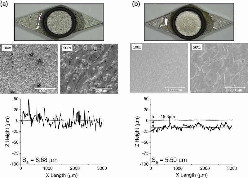
Fig. 7: Photos and profilometry line scans of AM 316L SS side skins before (as-printed) (A) and after (B) P/PR EP. Note, the as-printed photograph is the same image as that in the other side-by-side figures. This image is for visual comparison only. Also note, Sa values are from area scans, not line scans.
It is important to compare the type of roughness removed and difference in ΔM relative to DC EP. To make a rigorous comparison with DC EP with respect to roughness and ΔM, the coupon must be compared with a sample that was DC electroplated using the same amount of charge (− 7.5 A*min/cm2). Earlier, in “DC Electropolishing” section, the coupon used for the DC study underwent − 15 A*min/cm2 for comparison with a sample examined later in “Combining Pulse/Pulse Reverse and DC Electropolishing” section. When instead a sample was DC electroplated for − 7.5 A*min/cm2, the arithmetic mean height was slightly higher (Sa = 5.92 µm) than that for P/PR (5.50 µm) and resulted in an average thickness of 39 µm dissolved from the surface versus the 15 µm for P/PR EP. For DC EP, an iint,eff of 1 A*min/cm2 results in 4.1 mg of material removed. In contrast, an iint,eff of 1 A*min/cm2 using P/PR results in 1.6 mg of material removed. This could be due to the electrolyte used for P/PR (2.6 M NaCl/H2O) having different conductivity properties from the commercial EPS 2500 electrolyte (H3PO4/H2SO4) used for DC EP. Alternatively, it is likely that the charge delivered to the parts contributes to a linear combination of chemical reactions. In P/PR, larger overpotentials must be used to maintain the same ieff as DC. It is likely that these overpotentials are driving added reactions (e.g., water oxidation), which might contribute to the overall charge delivered, giving a higher apparent reduction in roughness per charge. This higher smoothing efficiency (i.e., more smoothing for less mass loss) for the P/PR and the ability to remove macro-asperities compared with DC EP offers the opportunity to better maintain part tolerances, especially when the two EP methods are combined into a two-electrolyte surface finishing strategy.
In contrast to DC EP, which relies on diffusion-limited processes at the near-surface, P/PR utilizes off-time to eliminate effects of diffusion, where the electric field is switched off before significant concentration gradients form and the tertiary current distribution increases. This converts P/PR to an exclusively primary/secondary current distribution process, where only the surfaces closest to the counter electrode are smoothed, regardless of asperity aspect ratio. This allows large features to be removed more selectively, whereas the smallest-sized asperities are smoothed more uniformly.
Combining Pulse/Pulse Reverse and DC Electropolishing
A two-electrolyte approach that combines the respective advantages of P/PR (macro-smoothing) and DC EP (micro-smoothing) was applied to a separate AM 316L SS coupon. Using the pulse parameters in Table III, the as-printed coupon was P/PR electroplated for iint,eff = − 7.5 A*min/cm2. The same coupon was then DC electroplated using the same methods described above (Sect. 3.1) for an additional iint,eff = − 7.5 A*min/cm2 (− 15 A*min/cm2 total). Sa and ΔM were measured before, in between, and after the P/PR and DC steps.
Figure 8 shows a comparison of an as-printed coupon and the coupon that underwent both P/PR and DC EP. As with the P/PR EP-only coupon, there was a considerable reduction in macro-asperity roughness, and the mirror-like finish is evidence that DC EP removed the micro-asperity roughness. The optical profilometry results support this conclusion. Most of the micro-asperity variation in the line scan has been removed, and the macro-asperities have also been reduced, compared with the as-printed coupon. When both polishing steps were combined, the Sa was reduced to an average of ~ 1.00 µm, with values ranging between 1.10 µm and 0.99 µm depending on where in the 1-cm2 circle the measurement was taken. The greater smoothing efficiency and macro-asperity selectivity of P/PR EP and micro-asperity selectivity of DC together yielded a smooth AM metal surface, comparable to machined surfaces from wrought products. The order of the P/PR and DC EP steps was also explored. We hypothesized that if P/PR is instead performed last, the final surface finish would have similar qualities to a P/PR-only EP sample (i.e., smooth, matte finish). Though primary current distribution dominates in P/PR, the current distribution still has some degree of uniformity, where most of the current focuses on the peaks closest to the counter electrode, and a small, non-zero amount of current etches surfaces in trenches. We thus expected P/PR to strip away mirror-like surfaces obtained from the initial DC. Nonetheless, we conducted the experiment confirming this, the final Sa was 3.0 µm and higher than the reverse order, which achieved 1.0 µm.
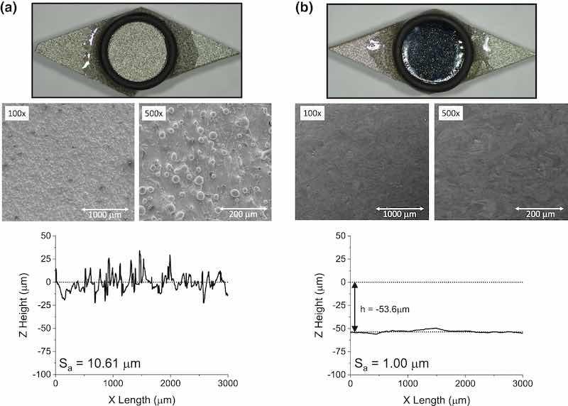
Fig. 8: Photos and profilometry line scans of AM 316L SS coupon side skins before EP (a) and after (b) the 2-step P/PR and DC EP. Note, the as-printed photograph is the same image as that in the other side-by-side figures. This is for visual comparison only. Also note, Sa values are obtained from area scans, not line scans.
Figure 9 shows a comparison of the best Sa values obtained for three samples, each having received 15.0 A*min/cm2 of charge by (1) DC-only, (2) P/PR-only, and (3) 2-Bath methods. Note the final surface roughness of the P/PR-only sample (4.1 µm). Despite its higher smoothing efficiency, the lowest obtainable roughness is not superior to the traditional DC method. As discussed above, this is likely due to more material being dissolved via DC as compared to P/PR for the same charge delivered. Higher overpotentials are used in the P/PR process to maintain the same ieff as DC, thus higher potentials are likely driving additional reactions, such as solvent oxidation.
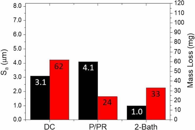
Fig. 9: A comparative plot showing the best Sa values (black) obtained by the DC-only, P/PR-only, and 2-Bath EP methods with the corresponding mass loss (red). Each sample received the same integrated effective current density of 15.0 A*min/cm2 (Color figure online).
Scale-Up
Electropolishing of larger, non-coupon parts was also accomplished using the two-electrolyte method. Figure 10 shows a full parallelogram sample (surface area = 16.8 cm2), which was electropolished using the same pulse and electrolyte parameters described in the methods Sections and Table III, where ipeak,anodic, ipeak,cathodic were scaled up by surface area. Here, the parallelogram sample was spot-welded to a SS wire and suspended in the center of a cylindrical counter electrode also made of 316L SS shim stock. The sample underwent − 7.5 A*min/cm2 of charge transfer by P/PR EP in the 2.6 M NaCl/H2O. The electrolyte was then replaced with EPS 2500 and DC electropolished for an additional − 7.5 A*min/cm2. The absolute Sa for the side-skin was reproduced successfully at 1.0 µm. The Sa for the up-skin, top-skin, and bottom-skin were 1.8 µm, 2.6 µm, and 2.0 µm, respectively. While some geometry change (e.g., rounded corners) occurs around the edges of the sample, where current densities are expected to be higher (due to being closer to the counter electrode), additional measures can be taken to mitigate non-uniform EP. The use of conforming counter electrodes to maintain constant distance between external surfaces and the counter electrode are a straightforward option for simpler-geometry components. For more complex shapes, the correlation of mass change and dissolving distance into the surface from fundamental studies, such as that presented above, could be used in combination with modeling software to anticipate non-uniform current distribution. Such models could be used to overprint high current density areas in anticipation of the preferentially dissolved material in localized areas.
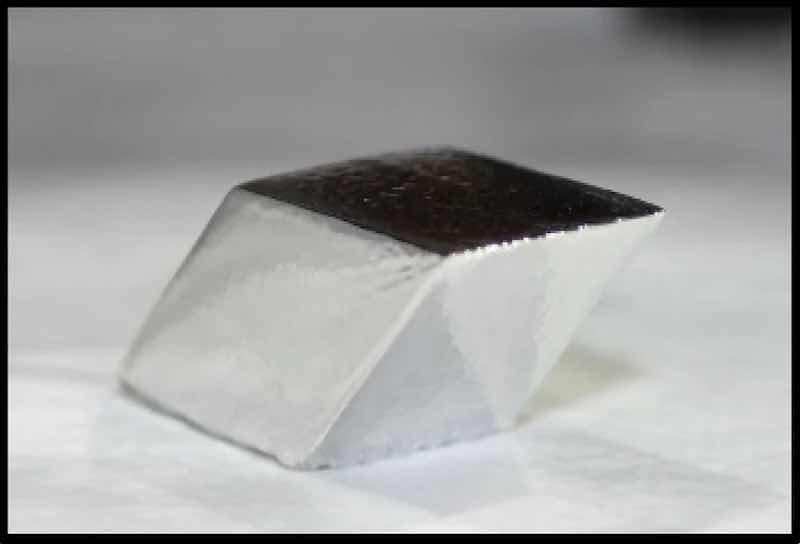
Fig. 10: Full AM 316L SS parallelogram sample after undergoing both P/PR and DC EP. Parallelogram surface area is 16.8 cm2. Sa were 1.0 µm, 1.8 µm, 2.6 µm, and 2.0 µm for the side-, up-, top-, and down-skins, respectively.
Minimizing Mass Loss
In many applications, minimizing mass loss might become necessary to preserve part geometry and meet required tolerances, with the goal to maximize reduction in surface roughness for the least change in mass/geometry. A series of experiments was carried out to explore the effects of EP duration (i.e., integrated effective current, iint,eff) on the amount of material removed and arithmetic mean height (Sa). Separate AM 316L SS coupons were P/PR electropolished in fresh 2.6 M NaCl/H2O at 1.5°C for increasing amounts of time [tEP in Eq. 4]: 60, 120 s, 240 s, 480 s, and 960 s (i.e., − 0.28 A*min/cm2, − 0.56 A*min/cm2, − 1.1 A*min/cm2, − 2.2 A*min/cm2, and − 4.4 A*min/cm2, respectively). The pulse parameters in Table III were used. Optical profilometry and mass measurements were performed for each coupon before and after the EP step.
Figure 11 shows the percent change in Sa and change in mass with increasing P/PR EP duration. Similar to Fig. 6, the percent change was reported to normalize any coupon-to-coupon variations from the initial surface roughness. Because ieff was held constant at − 0.281 A/cm2, a linear decrease in mass is expected with increasing iint,eff (charge transferred). Unlike coupon mass, the surface roughness adopts an exponential-like decay with increasing charge transfer (iint,eff). Thus, the most efficient EP occurs early in the process, with the largest amount of smoothing for the least amount of material removal. This type of study can be useful for predicting material removal rate in other materials as well.
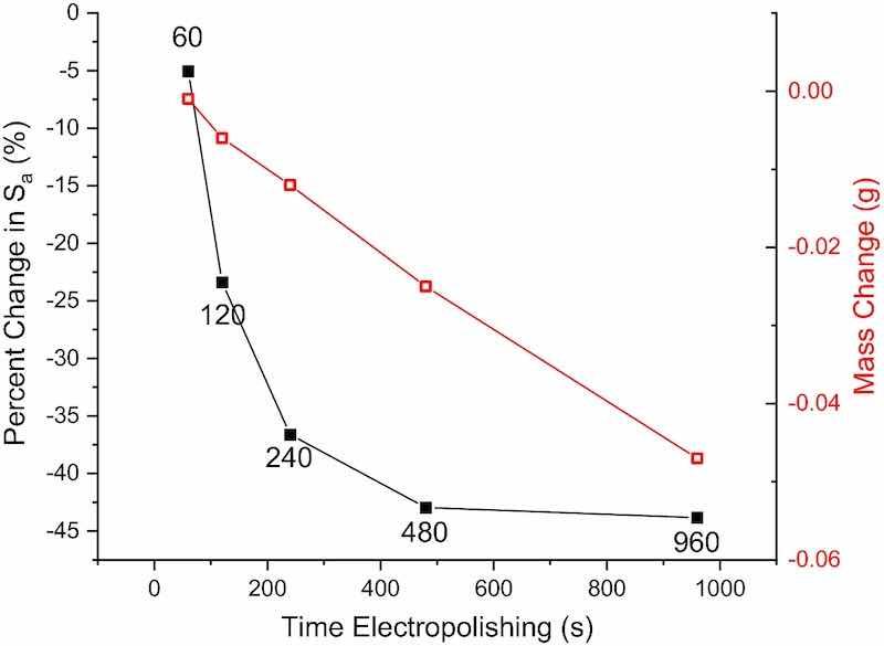
Fig. 11: Percent change in arithmetic mean height (Sa) and change in mass with increasing EP time (i.e., increasing iint,eff).
Conclusion
The work presented offers an explicit, effective, and scalable finishing method for smoothing AM 316L SS parts to Sa values as low as 1.0 µm. P/PR EP offers the unique ability to finely tune electrodynamic processes of the electrolyte allowing for the removal of wavy, macro-scale roughness features that DC EP has historically been unable to smooth. It was demonstrated that fundamental EP coupon studies are a useful tool for predicting the surface finish of larger parts. Pulse or electrolyte parameters can be varied, while accounting for changes in geometry due to mass loss. By carefully controlling parameters, such as effective and integrated effective currents, pulse sequences can be logically scaled up to accommodate larger components. While future work is being directed towards the development of pulse sequences capable of micro-smoothing (i.e., a single electrolyte method that can macro- and micro-smooth), the success of this method in macro-smoothing as an augmentation to existing DC EP methods offers a breakthrough towards the integration of AM 316L SS components into a wider range of applications with tighter restrictions on surface finish.
References
- J. Beaman, C. Atwood, T. Bergman, D. Bourell, S. Hollister, and D. Rosen. Additive/Subtractive Manufacturing Research and Development in Europe (World Technology Evaluation Center Inc, 2004) https://apps.dtic.mil/sti/pdfs/ADA466756.pdf. Accessed 06 Sept 2022
- C.Y. Yap, K. Chua, Z. Dong, Z. Liu, D. Zhang, L.E. Loh, and S.L. Sing, Appl. Phys. Rev. 2, 041101. https://doi.org/10.1063/1.4935926 (2015).
- T.D. Ngo, A. Kashani, G. Imbalzano, K.T.Q. Nguyen, and D. Hui, Compos. Part B 143, 172. https://doi.org/10.1016/j.compositesb.2018.02.012 (2018).
- N.S. Al-Mamun, W. Haider, and I. Shabib, Electrochim. Acta. 362, 137039. https://doi.org/10.1016/j.electacta.2020.137039 (2020).
- M.J.K. Lodhi, K.M. Deen, M.C. Greenlee-Wacker, and W. Haider, Addit. Manuf. 27, 8. https://doi.org/10.1016/j.addma.2019.02.005 (2019).
- P. Kumar, R. Jayaraj, J. Suryawanshi, U.R. Satwik, J. McKinnell, and U. Ramamurty, Acta Mater. 199, 225. https://doi.org/10.1016/j.actamat.2020.08.033 (2020).
- D. Gu, Laser Additive Manufacturing of High-Performance Materials (Springer, Berlin, 2015).
- J.P. Kruth, L. Froyen, J. Van Vaerenbergh, P. Mercelis, M. Rombouts, and B. Lauwers, J. Mater. Proc. Technol. 149(1), 616. https://doi.org/10.1016/j.jmatprotec.2003.11.051 (2004).
- P.J. Núñez, E. García-Plaza, M. Hernando, and R. Trujillo, Procedia Eng. 63, 771. https://doi.org/10.1016/j.proeng.2013.08.255 (2013).
- S. Kumar, A. Choudhary, A. Singh, and A. Gupta, Int. J. Innov. Res. Technol. Sci. Eng. 3, 147. (2016).
- A. Diaz, Additive Manufacturing for the Aerospace Industry (Elsevier, Amsterdam, 2019), pp 341–374.
- P. Tyagi, T. Goulet, C. Riso, R. Stephenson, N. Chuenprateep, J. Schlitzer, C. Benton, and F. Garcia-Moreno, Addit. Manuf. 25, 32. https://doi.org/10.1016/j.addma.2018.11.001 (2019).
- T.M. Mower and M.J. Long, Mater. Sci. Eng. A 651, 198. https://doi.org/10.1016/j.msea.2015.10.068 (2016).
- R. Shrestha, J. Simsiriwong, and N. Shamsaei, Addit. Manuf. 28, 23. https://doi.org/10.1016/j.addma.2019.04.011 (2019).
- A. Toma, R. Condruz, R. Carlanescu, and I. Daniel, AIP Conf. Proc. 2302(1), 060017. https://doi.org/10.1063/5.0033732 (2020).
- M.A. Melia, H.D.A. Nguyen, and J.M. Rodelas, Corros. Sci. 152, 20. https://doi.org/10.1016/j.corsci.2019.02.029 (2019).
- S.J. Lee and J.J. Lai, J. Mater. Proc. Technol. 140(1), 206. https://doi.org/10.1016/S0924-0136(03)00785-4 (2003).
- G. Selvaduray, S. Trigwell. Effect of surface treatment on surface characteristics and biocompatibility of AISI 316L stainless steel. Paper presented at ASME 2006 Frontiers in Biomedical Devices Conference, Irvine California 8–9 June 2006. https://doi.org/10.1115/NANOBIO2006-18031
- S. Yang and W. Li, Surface Finishing Theory and New Technology (Springer, Berlin, 2018).
- S. Bagehorn, J. Wehr, and H.J. Maier, Int. J. Fatigue 102, 135. https://doi.org/10.1016/j.ijfatigue.2017.05.008 (2017).
- A. Teixeira, Development of an Electropolishing Method for Titanium Materials (Concordia University, Montreal, 2011).
- P.A. Jacquet, Nature 135(3426), 1076. https://doi.org/10.1038/1351076c0 (1935).
- W.C. Elmore, J. Appl. Phys. 10(10), 724. https://doi.org/10.1063/1.1707257 (1939).
- W.C. Elmore, J. Appl. Phys. 11(12), 797. https://doi.org/10.1063/1.1712738 (1940).
- A. Chandra, M. Sumption, and G. Frankel, J. Electrochem. Soc. 159, C485. https://doi.org/10.1149/2.054211jes (2012).
- P. Tyagi, T. Goulet, C. Riso, K. Klein, and F. Garcia-Moreno. Electropolishing of Additively Manufactured High Carbon Grade 316 Stainless Steel (Engineering engrxiv Archive, 2018). https://doi.org/10.31224/osf.io/5dn49. Accessed 6 Sept. 2022
- L. Yang, H. Gu, and A. Lassell. Surface treatment of Ti6al4V parts made by powder bed fusion additive manufacturing processes using electropolishing. Paper presented at Solid Freeform Fabrication (SFF) Symposium, Austin Texas, 4–6 August 2014
- Y.C. Wu, C.N. Kuo, Y.C. Chung, C.H. Ng, and J.C. Huang, Materials 12(9), 1466. https://doi.org/10.3390/ma12091466 (2019).
- H. Garich and T. Hall, Electrochemical surface finishing of additively manufactured parts. ECS Trans. 85, 155. https://doi.org/10.1149/08504.0155ecst (2018).
- T. Hall, H. Garich, H. McCrabb, S. Snyder, and E. Taylor. Robust, HF free, and water based polishing and finishing processes for complex shapes. Paper presented at Materials Science and Technology 2016 Conference and Exhibition, Salt Lake City Utah, 23–27 Oct. 2016
- M. Inman, E. Taylor, and T. Hall, J. Electrochem. Soc. 160, E94. https://doi.org/10.1149/2.044309jes (2013).
- E. Taylor, Plat. Surf. Finish. 3(4), 178. (2008).
- M. E. Inman, H. Garich, S. Snyder, E. J. Taylor, L. D. Cooley, and A. M. Rowe. Development and scale-up of an HF-free electropolishing process in single-cell niobium SRF cavities. Paper presented at International Conference of RF Superconductivity, Chicago Illinois, 25–29 Jul. 2011
- A. Rowe. Bipolar EP: electropolishing without fluorine in a water based electrolyte. Paper presented at International Conference of RF Superconductivity, Paris France, 22–27 Sept. 2013
- C. Zhou, E. J. Taylor, J. J. Sun, L. E. Gebhart, and R. P. Renz. Electrochemical Machining Using Modulated Reverse Electric Fields. US6402931B1 (2002)
- E. J. Taylor. Sequential electromachining and electropolishing of metals and the like using modulated electric fields. US6558231 (2003)
- E. J. Taylor, M. E. Inman, and T. Hall. Electrochemical System and Method for Electropolishing SCRF Cavities. US9006147 (2015)
- W. Han and F. Fang, Int. J. Mach. Tools Manuf. 139, 1. https://doi.org/10.1016/j.ijmachtools.2019.01.001 (2019).
- M.E. Inman, E.J. Taylor, and T.D. Hall, J. Electrochem. Soc. 160(9), E94. https://doi.org/10.1149/2.044309jes (2013).
- E. Taylor, H. McCrabb, H. Garich, T. Hall, and M. Inman. A pulse/pulse reverse surface finishing for electropolishing and through mask electroetching (Products Finishing, 2012). https://www.pfonline.com/articles/a-pulsepulse-reverse-electrolytic-approach-to-electropolishing-and-through-mask-electroetching. Accessed 6 Sept. 2022
- E. J. Taylor, T. D. Hall, M. E. Inman, S. Snyder, and A. M. Rowe. Electropolishing of niobium SRF cavities in low viscosity aqueous electrolytes without hydrofluoric acid. Paper presented at International Conference of RF Superconductivity, Paris France, 22–27 Sept. 2013
- E. Taylor, M. Inman, H. Garich, H. McCrabb, S. Snyder, and T. Hall. Advances in Electrochemical Science and Engineering (Wiley-VCH, 2018) pp 193–239. https://doi.org/10.1002/9783527807215.ch7
- M. E. Inman, E. J. Taylor, and O. Trofimova. Niobium electropolishing in an aqueous, non-viscous HF-free electrolyte: a new polishing mechanism. Paper presented at International Conference of RF Superconductivity, Chicago Illinois, 25–29 Jul. 2011
- Z. Chaghazardi and R. Wüthrich, J. Electrochem. Soc. 169(4), 043510. https://doi.org/10.1149/1945-7111/ac6450 (2022).
- C. Wagner, J. Electrochem. Soc. 101(5), 225. https://doi.org/10.1149/1.2781235 (1954).
Acknowledgements
We are grateful to Colt Montgomery, Robbin Pacheco, and Michael Brand for performing sample preparation. We would also like to thank Zachary Koehn for his assistance in acquiring scanning electron microscopy images. This work was supported by the Los Alamos National Laboratory Office of Engineering and Technology Maturation. Work was performed, in part, at the Center for Integrated Nanotechnologies, an Office of Science User Facility operated for the U.S. Department of Energy (DOE) Office of Science. The U.S. Department of Energy (Contract 89233218CNA000001) supported this work.
Author information: Authors and Affiliations: Sigma Manufacturing Sciences Division, Los Alamos, NM, USA: Timothy J. Gorey, Jamie A. Stull, Robert E. Hackenberg, Courtney L. Clark and Daniel E. Hooks
Center for Integrated Nanotechnologies, Los Alamos National Laboratory, Mailstop G774, PO Box 1663, Los Alamos, NM, 87545, USA: Daniel E. Hooks
Contributions: TJG: lead investigator, conceptualization, methodology, experimentation, data acquisition and analysis, author of original draft, draft review, and editing. JAS: project principal investigator, funding acquisition, conceptualization, methodology, draft review, and editing. REH: methodology, draft review, and editing. CLC: draft review and editing. DEH: team lead/manager, conceptualization, methodology, draft review, and editing.
Ethics declarations: Competing interest: All authors declare that there are no competing financial interests or personal relationships that could influence work reported in this paper.