


This paper focuses on the application of pulse/pulse reverse (P/PR) electrolytic processes to problems of relevance to the surface finishing industry.
 E. Jennings Taylor, PhD.After a brief introduction to the concept and principles of P/PR electrolysis, I discuss the importance of electrolytic cell design in establishing a uniform hydrodynamic boundary layer. I then focus on past developments and current applications of P/PR electrolysis at Faraday Technology, including (1) cathodic processes for electrodeposition and electrophoretic deposition, (2) anodic processes for electrodeburring, electropolishing and electroetching and (3) processes for electro-assisted ion exchange.
Note: This piece was written at the time Dr. Taylor was announced as the recipient of the 2007 Scientific Achievement Award by the NASF.
Introduction
My first introduction to P/PR electrolysis was as a graduate student while conducting my dissertation research at Brookhaven National Laboratory and I first begin working in the area while employed at Physical Sciences Inc. From these initial forays, I had the good fortune and family support to found Faraday Technology, Inc. in 1991, whose audacious vision was and still is:
“...to be known as the company that changed the focus of electrochemical technologies from the art of complex chemistries to the science of P/PR electric fields...”
Our approach has been coined “Electrochemical Magic of a Different Kind.”1
 Figure 1 - Cell geometry as the foundation for electrolytic process development.At Faraday, we have the freedom to explore our vision for P/PR electrolysis, as long as we can convince people to fund our ideas for their applications. The quid pro quo to commercial company funding is that in return, they have the exclusive rights associated with the P/PR developments. Consequently, intellectual property in the form of patents and know-how plays an important part in our strategy and I cite them below as appropriate. After seventeen years of commercial and government- sponsored research, twenty-one issued U.S and five foreign patents, numerous licensees and following the acquisition of Faraday by Physical Sciences, I am pleased to say the vision is indeed alive and well!
Although the focus of our activities is the development of P/PR electrolysis processes, an important and often forgotten consideration is the design of the electrolytic apparatus or cell. As depicted in Fig. 1, the cell geometry is the foundation of our process development. In fact, I submit that cell design considerations are often neglected when evaluating process parameters and a poor cell design often overshadows an otherwise superior process.
Critical to our development of P/PR electrolytic process parameters was the seminal work by Puippe and Leaman, published by the American Electroplaters and Surface Finishers Society, The Theory and Practice of Pulse Plating.2 Although out of print, several well-worn copies of this tome grace the Faraday laboratories.
Since the combination of P/PR electrolysis waveforms to achieve a given average current density is infinite, over the years we have developed some simplifying assumptions and guiding principles regarding the development of P/PR electrolysis applications.
P/PR Electrolysis: Guiding Principles
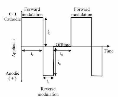 Figure 2 - Generic representation of P/PR electrolysis waveform.As shown in Fig. 2, the generalized P/PR waveform consists of a forward modulation (shown as cathodic) with a cathodic current density, ic, a cathodic on time, tc, a reverse modulation (shown as anodic) with an anodic current density, ia, an anodic on time, ta, and an off-time, t0. Note, an additional off time between the forward and reverse modulation is not depicted for simplicity. The sum of the cathodic and anodic on-times and the off-time is the period, T, of the modulation and the inverse of the period is the frequency, f, of the modulation. The cathodic, ¡c, and anodic, ¡a, duty cycles are the ratios of the respective on-times to the charge modulated period. The average current density (iaver) or net electrodeposition rate is given by:
iaver = ic¡c - ia¡a (1)
Just as there are infinite combinations of height, width, and length to obtain a given volume, in P/PR processes there are unlimited combinations of peak current densities, duty cycles and frequencies to obtain a given electrolysis rate. These additional parameters provide the potential for much greater process/product control versus DC plating.
Mass transport in P/PR electrolysis is a combination of steady state and non-steady state diffusion processes. Cheh and coworkers3,4 previously discussed the theory of mass transport with respect to pulse electrolysis. In steady state DC electrolysis, δ is a time-invariant quantity for a given electrode geometry and hydrodynamic conditions. In P/PR electrolysis, however, δ varies from 0 at the beginning of the pulse to its steady state value, when the Nernst diffusion layer is fully established. The corresponding diffusion limiting current density would then be equal to an infinite value at t = 0 and decreases to a steady state value of the DC limiting current density. The advantage of P/PR electrolysis is that the current can be interrupted before δ has a chance to reach the steady-state value. This allows the reacting ions to diffuse back to the electrode surface and replenish the surface concentration to its original value before the next current modulation. Therefore, the concentration of reacting species in the vicinity of the electrode pulsates with the frequency of the modulation.
Under pulse electrolysis, Ibl and colleagues5,6,7 proposed a “duplex diffusion layer” consisting of a pulsating layer, δp, and a stationary layer, δs. Modeling work by Landolt has also suggested the existence of a pulsating diffusion layer.8 Since the thickness of the pulsating diffusion layer is determined by the waveform parameters, we call this layer the “electrodynamic diffusion layer.”9 By assuming a linear concentration gradient across the pulsating diffusion layer and conducting a mass balance, Ibl derived the pulsating diffusion layer thickness (δp) as:6
δp = (2Dton)1/2 (2)
and when the pulse on-time is equal to the transition time, τ, the concentration of reacting species at the interface drops to zero precisely at the end of the pulse:
T = ((nF)2 Cb 2D)/2ic2 (3)
More recently, Yin,10 using a similar approach as Ibl, derived the same equation for the pulsating diffusion layer for “pulse-with- reverse” plating.
The key points used in our development of a P/PR electrolysis process are (1) the electrodynamic diffusion layer thickness is proportional to the pulse on-time, and (2) the transition time is inversely proportional to the current. Further, note that the on time is directly proportional to the duty cycle and inversely proportional to the frequency.
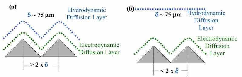 Figure 3 - Under pulse electrolysis: (a) Macroprofile converted to a smaller macroprofile and (b) Microprofile converted to a macroprofile.
We consider two additional important aspects when designing a P/PR electrolysis process. The first is whether the current distribution is controlled by primary (geometrical), secondary (kinetic) or tertiary (mass transport) considerations. For example, if the waveform is designed so that the pulse on time is much longer than the transition time, the tertiary current distribution will be an important factor in metal distribution. The addition of kinetic or tertiary effects tends to make the current distribution more uniform, as compared to primary current distribution.
 Figure 4 - (a) Schematic diagram of an electrolytic cell facilitating uniform laminar flow and (b) photo of the operating unit.When tertiary current distribution effects are important, additional criteria that influence current distribution are the concepts of macroprofile and microprofile. In a macroprofile, the roughness of the surface is large compared with the thickness of the diffusion layer, and the diffusion layer tends to follow the surface contour. Under mass transport or diffusion control, a macroprofile results in a uniform current distribution or a conformal deposit during plating. In a microprofile, the roughness of the surface is small compared with the thickness of the diffusion layer. As shown in Figs. 3a and b, pulse electrolysis can convert a macroprofile to a smaller macroprofile and a microprofile to a macroprofile, respectively.
Our final “guiding principle” regarding the exploration of applications for P/PR electrolysis involves strict application of the scientific method by testing assumptions. Specifically, much of the prior art, P/PR electrolysis took process chemistries developed for direct current (voltage) processes and applied pulse waveforms. However, we asked two questions:
- Why should we expect P/PR electrolysis processes to use the same chemistries in terms of electrolytes and additives as those developed for DC processes?
- In fact, do P/PR electrolysis processes require anything more than simple electrolyte and additive chemistries?
Consequently, our approach to the exploration of P/PR electrolysis applications begins with simple electrolytes and easy to control additives.
Electrolytic Cell for Uniform Hydrodynamic Boundary Layer
As noted above, the design of the electrolytic apparatus is critical to the development of P/PR processes, as well as conventional process technology. Masking is an important geometric consideration for electrolytic apparatus design and we presented a simple model for guidance.11 In addition, conventional agitation approaches typically use air/inert gas sparging or eductors impinging on the workpiece with coefficients of variation of 14% and 18%, respectively, for a rectangular workpiece of 450 × 600 mm.12
A design developed at Faraday utilizes eductors to avoid the issues associated with non-uniform gas bubble size in sparging approaches. However, in our approach, the eductor flow does not directly impinge upon the workpiece as shown in Fig. 4.13,14 With this flow scheme, we have demonstrated coefficient of variation of 4% to 5% for 200 mm wafer package and 450 × 600 mm circuit board substrates, respectively. In addition, we have measured boundary layers approaching 10 μm in thickness using limiting current measurements.
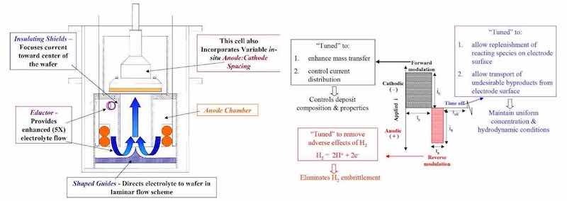 Figure 5 - Wafer plating tool with rotation and vertical move; Figure 6 - Generalized pulse/pulse reverse waveform for ment.
Another design for horizontal electrolytic processes uses a rotating wafer with vertical movement to compensate for terminal effects due to a minimally conductive seed layer.15 For this design, shown in Fig. 5, we demonstrated coefficient of variation of 4 to 6% and a boundary layer thickness of ~34 μm.16
P/PR Cathodic Electrodeposition Processes
Figure 6 depicts a generalized P/PR electrolysis waveform for electrodeposition applications where the “forward” cycle is cathodic and the “reverse” cycle is anodic and the net process is cathodic. In addition to the current distribution issues discussed above in terms of macro and microprofiles and the electrodynamic boundary layer, we tune the P/PR waveform reverse (anodic) cycle to consume the nascent hydrogen generated in many cathodic processes. As discussed below, this is an important enabling function of P/PR electrolysis for certain applications.
 Figure 7 - P/PR electrolysis related to interconnects for electronic applications.An initial application we investigated for P/PR electrolysis involved metallization of interconnects for printed circuit boards and electronic packages. The main challenge for these applications is controlling the current distribution in order to prevent “dog-boning,” i.e., to obtain good throwing power. While throwing power is generally addressed using plating baths containing difficult-to-control additives such as levelers and brighteners, we used the P/PR waveform to control the throwing power. As shown in Fig. 7 for the test panel with various features, we obtained good throwing power for plated through holes and pattern plating over a range of feature sizes. Our approach generally used the concepts described above for microprofile and macroprofile boundary layers and tuning the forward (cathodic deposition) and reverse (anodic dissolution) waveform characteristics in order to yield the net result of conformal coating or filling of the subject interconnects.17,18 Another advantage of P/PR electrolysis is that for electronic packages having different feature sizes, a sequence or train of waveforms can be delivered to address the range of features.19,20,21
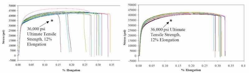 Figure 8 - Stress-strain curves for copper samples prepared using (a) a conventional additive chemistry process at NSWCCrane and (b) P/PR with a simple chemistry.
Another important property of P/PR electrolysis related to electronic packages is the ductility of the resulting deposit. In Fig. 8, we present stress/strain data for copper foils prepared from a commonly used chemical additive bath using a conventional process at the Naval Surface Warfare Center - Crane (NSWC-Crane) Indiana and data from a simple chemical bath using a P/PR waveform sequence developed at Faraday. We observed equivalent yield strength and elongation with the P/PR prepared samples showing a standard deviation of ~2% for elongation compared to ~6% for the conventionally prepared samples.22 We demonstrated the versatility of P/PR electrolysis with semiconductor applications where the feature sizes are typically less than 0.25 μm and microprofile boundary layers are typically operative. A representative set of results is presented in Fig. 9.23-28
 Figure 9 - P/PR electrolysis related to interconnects for semiconductor electronic applications.Another application for P/PR electrolysis is the electrodeposition of thick chromium coatings from an environmentally-friendly trivalent chromium plating bath. Current processes for trivalent chromium are limited to thin decorative applications. We speculated that this was due to the cathodic generation of hydrogen during trivalent chromium plating. Based on this assumption, we successfully demonstrated that we could plate thick chromium coatings from trivalent baths using P/PR electrolysis. We speculate that the reverse (anodic) cycle consumes the nascent hydrogen and allows the deposition to continue.29-32 Although the chromium deposits prepared from P/PR electrolysis had a thickness equivalent to those from a standard hexavalent chromium bath, we observed poor properties in terms of wear and corrosion resistance. From cross-section data, we attributed these poor properties to continuous cracks through the coating to the substrate surface. Although chromium prepared from hexavalent processes also exhibits cracks, they are they discontinuous. Consequently, we used a looping P/PR waveform in order to interrupt the electrodeposition process with the idea of eliminating or reducing the contiguous cracks. In this manner, we demonstrated a significant reduction in contiguous cracks, as shown in Figure 10.33,34
Another application of P/PR waveform looping is related to tin electrodeposits as a lead-free solder. We previously demonstrated that various P/PR waveforms yield either tensile or compressive internal stress as well as different magnitudes of said stress.35 Since internal stress is attributed to whisker growth in lead-free tin solders, we investigated several P/PR waveform sequences to generate layered tin deposits with different types and magnitudes of internal stress.36 Preliminary data from thermal cycling indicate that depositing successive layers of different internal stress is a promising approach for mitigation of whisker growth in tin electrodeposits.
 Figure 10 - Comparison of continuous and discontinuous cracks during DC chrom- ium plating from a hexavalent chromium plating bath and from a trivalent chromium bath without and with P/PR looping.In a totally different application of P/PR electrodeposition, we demonstrated the feasibility of preparing platinum electrocatalysts for fuel cell gas diffusion electrodes.37,38
Using the P/PR process we demonstrated the ability to form 3 to 4-nm catalyst particles with improved performance and the same loading of conventionally prepared electrocatalysts.39 Another P/PR application we are exploring is the fabrication of three- dimensional structures for microelectromechanical systems (MEMS).40
Thus far, I have described electrodeposition of metals from a plating bath containing ions of said metal. More recently, we are exploring the electrophoretic deposition of mixed oxides, specifically yittria-stabilized zirconia. We are investigating electrophoretic deposition of mixed oxides for applications such as thermal barrier coatings for turbine engines or varactor devices for RF filters, which are currently deposited using thermal spray or pulsed laser deposition, respectively. Electrophorectic deposition offers the benefits of speed and the ability to coat contoured surfaces. We are observing benefits of P/PR electrophoretic deposition and the ability to control coating morphology as shown in Fig. 11.41,42,43
P/PR Anodic (Electropolishing, Electrodeburring, Electroetching) Processes
 Figure 11 - Surface morphology of yittria-stabilized zirconia coatings prepared using P/PR electrophoretic deposition.Figure 12 depicts a generalized P/PR electrolysis waveform for electropolishing, electrodeburring and electroetching applications where the “forward” cycle is shown as anodic, the “reverse” cycle is shown as cathodic and the net process is anodic. For P/PR electrolysis anodic applications, we tune the reverse cycle to remove surface oxides for certain materials and alloys in order to “activate” the surface for the anodic cycle.44In addition to activating the surface, we tune the waveform using the concepts of electrodynamic boundary layer and macro-and microprofiles to focus the current distribution for electropolishing, electrodeburring and electroetching applications.
In Fig. 13, we present several exemplary electrodeburring applications using P/PR electrolysis. The planetary gear is made from tool steel and there was no need for a reverse cycle to remove the oxide and “activate” the surface. However, the blade was made from stainless steel and a reverse cycle was used.45 In Fig. 14, we present a P/PR application that we are developing for removing molehills and radiusing leading/trailing edges of an aerospace integrally-bladed rotor. Of particular note is that by proper selection of the P/PR waveform parameters, we can achieve a radius, taper or nearly complete removal of artifacts resulting from prior processing. The materials investigated to date include nickel and titanium based alloys.46
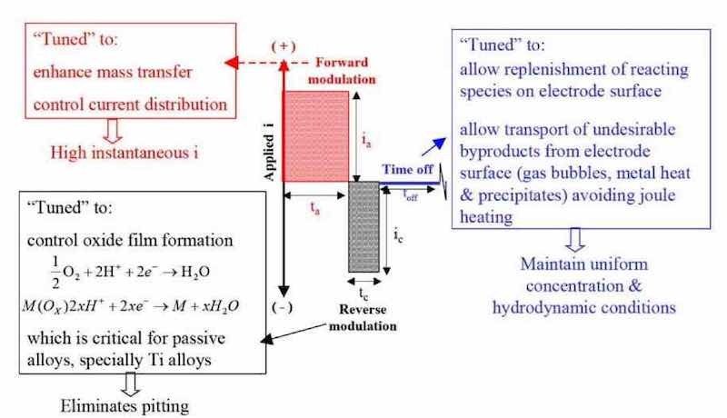 Figure 12 - Generalized pulse/pulse reverse waveform for anodic processes – electropolishing, electrodeburring and electroetching.
 Figure 13 - Electrodeburring applications using forward pulse; Figure 14 - P/PR electrolysis applied to aerospace compo- electrolysis. In Fig. 15, we present several P/PR electropolishing applications related to various stainless steel parts.47 An important consideration during P/PR electropolishing applications is that at the beginning of the process, the boundary layer may represent a macroprofile but as electropolishing continues a microprofile may evolve. To compensate for this change from macroprofile to microprofile, we use a sequence of P/PR waveforms to continue the electropolishing to the desired surface finish.48 We are currently investigating additional P/PR electrolysis applications related to small parts and medical devices.49,50 Another application involves using P/PR electrolysis to prepare or “activate” a passive surface for subsequent electrodeposition.51
In Fig. 16, we present an example of P/PR electroetching through a mask on a substrate. P/PR electroetcthing applications include substrates consisting of a metal layer on a non-conductive layer (electronic packages)52or substrates consisting solely of a metal layer (bipolar plates, microchannel reactors, microfluidic devices, cooling channels and the like). By tuning the P/PR waveform to focus the electric field, we minimize the mask undercut associated with isotropic nature of the chemical etching process.53 We are exploring other applications of P/PR electrolysis including removal of sacrificial cores for internal channels54,55 and removal of excess metal plating for semiconductor applications.56
 Figure 15 - P/PR electropolishing of stainless steel components; Figure 16 - P/PR through-mask electroetching.
Pulsed-Assisted Ion Exchange
 Figure 17 - P/PR-assisted ion exchange for treatment and regeneration of metal finishing process streams.In Fig. 17, we present a schematic representation of pulsed assisted ion exchange for the treatment and regeneration of metal finishing process streams.57,58 Pulsed assisted ion exchange addresses several key limitations associated with traditional ion exchange. During the treatment cycle, the pulsed electric field enhances the ionic transport to the anion and cation exchange resin beds. During the regeneration cycle, the pulsed electric field enhances the regeneration of the anion and cation resin beds without the need for strong acid or base process streams.59 Although illustrated for copper rinse waters, we believe pulsed- assisted ion exchange is applicable to a wide range of process streams related to the surface finishing and nuclear industries.
Concluding Remarks
My hope is that our collective body of work provides the basis for continued innovation related to the application of P/PR electrolysis to the electrochemical arts. I strongly believe that although our innovations to date are significant, we have only exposed the tip of the iceberg of possibilities related to P/PR electrolysis.
In addition, I recommend that we as scientists, technologists and researchers continue to revisit and test our assumptions. Additionally, I submit that the patent literature is a valuable source of technical information and should be reviewed just as more traditional sources of technical information are consulted.
Finally, I strongly encourage the use of collaborative teams where all viewpoints and ideas are considered in order to encourage creative thinking and innovation.
E. Jennings Taylor, PhD., is Principal at Faraday Strategies. Previously he was Chief Technical Officer and Intellectual Property Director at Faraday Technology Inc., an electro-chemical engineering company that he founded in 1991. This piece was written at the time Dr. Taylor was announced as the recipient of the 2007 Scientific Achievement Award by the NASF.
References
1. J.H. Lindsay, Ed., Plating & Surface Finishing, 90 (11), 18 (2003).
2. J-C. Puippe & F. Leaman, Theory and Practice of Pulse Plating, NASF, Washington, DC, 1986.
3. H.Y. Cheh, J. Electrochem. Soc., 118 (7), 551 (1971); ibid., p. 1132.
4. K. Viswanathan, M.A. Farrell-Epstein & H.Y. Cheh, J. Electrochem. Soc., 125 (11), 1772 (1978).
5. N. Ibl, J.C. Puippe & H. Angerer, Surface Technology, 6 (4), 287 (1978).
6. N. Ibl, Surface Technology, 10 (2), 81 (1980).
7. N. Ibl, Proc. 2nd International Pulse Plating Symposium, NASF, Washington, DC (1981).
8. D. Landolt, “Mass Transport in Pulse Plating” in Theory and Practice of Pulse Plating, J-C. Puippe & F. Leaman, Eds., NASF, Washington, DC, 1986; pp. 55-71.
9. E.J. Taylor, et al., Plating & Surface Finishing, 89 (5), 88 (2002).
10. K. Yin, Surface and Coatings Technology, 88 (1-3), 162 (1996).
11. A. Lozano-Morales, et al., Plating & Surface Finishing, 95 (3), 34 (2008); also J. Applied Surface Finishing, 3 (1), 36 (2008), online thru www.nasf.org.
12. H. Garich, et al., ECS Trans., 3 (16), 1 (2007).
13. L. Gebhart, et al., U.S. Patent Application 10/804,841, March 19, 2004.
14. L. Gebhart & E.J. Taylor, U.S. Patent Application 11/836,903, August 10, 2007.
15. J-M. Lee, et al., J. Electrochem. Soc., 153 (4), C265 (2006).
16. H. McCrabb, et al., ECS Trans., 6 (8), 185 (2007).
17. E.J. Taylor, J. Sun & C. Zhou, U.S. Patent 6,210,555, April 3, 2001.
18. E.J. Taylor & J. Sun, U.S. Patent 6,827,833, December 7, 2004.
19. E.J. Taylor, J. Sun & Inman, U.S. Patent 6,309,528, October 30, 2001.
20. E.J. Taylor, J. Sun & M. Inman, U.S. Patent 6,652,727, November 25, 2003.
21. E.J. Taylor, J. Sun & M. Inman, U.S. Patent 6,863,793, March 8, 2005.
22. H. Garich, et al., "Effects of Plating Cell Configuration on the Quality of Copper Deposits for Printed Circuit Boards", Presented at IPC Printed Circuits Expo, APEX and the Designers Summit, February 5-10, 2006, Anaheim, CA.
23. E.J. Taylor, C. Zhou & J. Sun, U.S. Patent 6,203,684, March 20, 2001.
24. E.J. Taylor, J. Sun & C. Zhou, U.S. Patent 6,303,014, October 16, 2001.
25. E.J. Taylor, C. Zhou & J. Sun, U.S. Patent 6,319,384, November 20, 2001.
26. E.J. Taylor, J. Sun & C. Zhou, U.S. Patent 6,524,461, February 25, 2003.
27. E.J. Taylor, U.S. Patent 6,750,144, June 15, 2004.
28. E.J. Taylor, C. Zhou & J. Sun, U.S. Patent 6,878,259, April 12, 2005.
29. R. Renz, et al., Plating & Surface Finishing, 90 (6), 52 (2003).
30. R. Renz, et al., J. Applied Surface Finishing, 1 (2) 155 (2006).
31. A. Lozano-Morales, et al., J. Applied Surface Finishing, 2 (3), 185 (2007).
32. A. Lozano-Morales, et al., ECS Trans., 6 (9), 51 (2007).
33. A. Lozano-Morales, M. Inman & E.J. Taylor, Meeting Abstracts, Electrochem. Soc., 801, 872 (2008); paper accepted for publication: ECS Trans., 16, (2008).
34. P. Chalmer, et al., U.S. Patent Application 11/501,551, February 21, 2008.
35. H. Garich, et al., ECS Trans., 6 (8), 153 (2007).
36. E.J. Taylor & J.J. Sun, U.S. Patent Application 11/620079, July 12, 2007.
37. N.R.K. Vilambi, E. Anderson & E.J. Taylor, U.S. Patent 5,084,144, January 28, 1992.
38. E.J. Taylor & M. Inman, U.S. Patent 6,080,504, June 27, 2000.
39. E.J. Taylor, E. Anderson & N.R.K. Vilambi, J. Electrochem. Soc., 139 (5), L45 (1992).
40. E.J. Taylor, U.S. Patent 6,551,485, April 22, 2003.
41. J. Kell, H. McCrabb & B. Kumar, “Faradayic Process for Electrophoretic Deposition of Thermal Barrier Coatings,” in Advanced Processing and Manufacturing Technologies for Structural and Multifunctional Materials II: Ceramic Engineering and Science Proceedings, T. Ohji & M. Singh, Eds., 29 (9), Wiley, Hoboken, NJ, 978-0-470-34499-6, to be published December 2008.
42. J.W. Kell, H.A. McCrabb & B. Kumar, Proc. Materials Science and Technology 2008 Conference, ASM International, Materials Park, OH, accepted June 2008.
43. J.W. Kell & H.A. McCrabb, “Faradayic Process for Electrophoretic Deposition of Thermal Barrier Coatings for use in Gas Turbine Engines,” Proc. American Ceramic Societies Fall Meeting at the Materials Science and Technology 2008 Conference, Ceramic Transactions, The American Ceramic Society, Westerville, OH, submitted September 2008.
44. J. Sun, E.J. Taylor & R. Srinivasan, J. Materials Processing Technology, 108 (3), 356 (2001).
45. J. Sun, et al., Proc. North American Manufacturing Research Conference XXVII, SME, Dearborn, MI, Product ID: TP00PUB112.
46. Privately funded activity for a commercial client, 2008.
47. C. Zhou, et al., U.S. Patent 6,402,931, June 11, 2002.
48. E.J. Taylor, U.S. Patent 6,558,231, May 6, 2003.
49. A. Lozano-Morales, et al., J. Applied Surface Finishing, 2 (3), 192 (2007).
50. A. Lozano-Morales, et al., Metal Finishing, 106 (3), 27 (2008).
51. A. Lozano-Morales, et al., Plating & Surface Finishing, 95 (10), 28 (2008); also J. Applied Surface Finishing, 3 (4), 163 (2008).
52. J. Sun, et al., Circuitree, pp. 12-17 (March 2006);
53. E.J. Taylor, J. Sun & H. McCrabb, U.S. Patent Application 11/354,376, February 15, 2006.
54. L. Gebhart, U.S. Patent 6,221,235, April 24, 2001.
55. L. Gebhart, U.S. Patent 6,676,825, January 13, 2004.
56. E.J. Taylor & H. Dyar, U.S. Patent 7,022,216, April 4, 2006.
57. E.J. Taylor, et al., U.S. Patent 5,599,437, February 4, 1997.
58. C. Zhou, et al., U.S. Patent 5,804,057, September 8, 1998.
59. H. Garich, et al., Plating & Surface Finishing, 91 (4), 36 (2004).