
Compact high-power density, high-efficiency, and low cost have been desired for power modules and high temperature operation reliability has been required for all materials for power modules and bonding interfaces.1
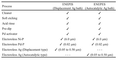 Table 1. Plating process of ENEPIS and ENEPESBecause operating temperatures became higher as chip materials changed from Si to SiC, the material for die attachment has been especially focused on. As the material for die attachment, Ag sinter is one of the leading candidates because of the desire to remove lead for environmental measures, superior electric conductivity and thermal conductivity, and higher melting temperature after sintering.2 There are pressure-assisted and pressure-free methods used for Ag sintering. It’s widely known that the Ag deposit has good reliability with Ag sintering material when using the pressure-free method, which isn’t affected by warpage and the steps of bonding surface.3,4
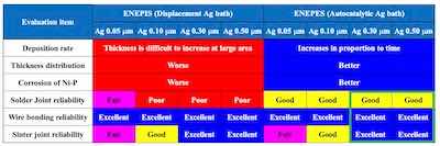
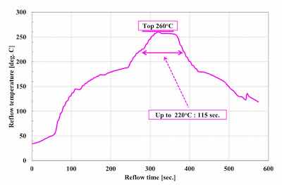 Figure 1. 260°C top severe reflow profile.Generally, Ag deposits for the chip backside have been formed by a sputter coating process.5 In this report, we confirmed the possibility of electroless Ag plating, which can process both sides at the same time. Solder joint reliability for the top side and Ag sintering joint reliability for the backside were evaluated for electroless Ni-P/electroless Pd- P/immersion Ag with displacement reaction (ENEPIS) and electroless Ni-P/electroless Pd-P/immersion Ag with autocatalytic reaction (ENEPES), compared with electroless Ni-P/electroless Pd-P/immersion Au with mixed reaction (ENEPIG). It was confirmed that ENEPES with a Ag thickness of 0.3 μm had good reliability both for the solder joint and Ag sintering joint. In the future, thermal cycle test after Ag sintering will be examined.
Introduction
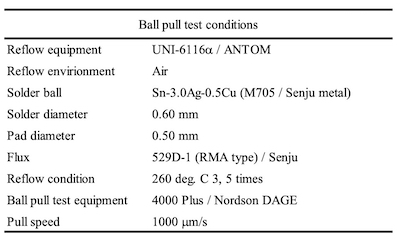 Table 2. Ball pull test conditionsThe characteristics of Ag metal are higher electrical conductivity, higher thermal conductivity, and higher reflectance in comparison to other metals. Due to these characteristics, it has been used for the metallization of connectors, leadfremes, waveguides, wiring of solar cells, reflector of LEDs, etc.6-10
In recent years, many researches have focused especially on Ag layers for the joint with Ag sinter materials in power modules, because it is known that the Ag sintering joint reliability between Ag sinter material and the Ag layer is good.2 There are many methods of Ag metallization such as sputtering, electrolyitc plating, and electroless plating with a displacement reaction.11
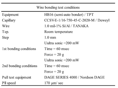 Table 3. Wire bonding test conditionsHowever, few studies of electroless Ag plating with autocatalytic reaction have been reported because it is difficult to control an electroless Ag bath continuously.12 In this report, the Ag sintering joint reliability of an electroless Ag deposit by autocatalytic reaction was compared with that of an electroless Ag deposit by displacement reaction. Additionally, thickness distribution, solder joint reliability (SJR), and wire bonding reliability (WBR) of each Ag deposit were evaluated.
Experimental Methods
For the Ag sintering joint reliability tests, base Cu material and Cu block were used. Base Cu material is used as a pseudo DBC substrate. Cu block is used as a pseudo chip. Uyemura test boards A and B used in this study consisted of a copper-clad laminated substrate which was copper plated to a thickness of 20 μm using an acid copper electrolytic plating process.
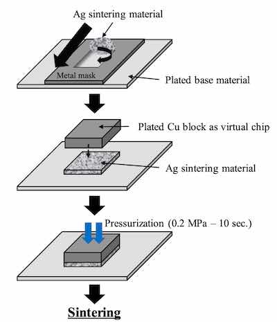 Figure 2. Evaluation method of the Ag sintering joint reliability test For the comparison of thickness distribution, Uyemura test board A was used. It has small pads of 1 x 2 mm and several big pads. 5 small pads are connected to backside pads by through holes. The area ratios between small pad and big pad of back side are 1:1, 1:10, 1:100, 1:1000 and 1:2000. The remaining small pads are not connected. For SJR tests, Uyemura test board B was used. The copper-plated area was coated with solder mask and imaged to form solder ball pads of 0.5 mm diameter. Both substrates were plated with ENEPIS and ENEPES by using plating chemicals commercially available from C. Uyemura & Co., Ltd.. Table 1 shows the plating process of ENEPIS and ENEPES. The thicknesses of each deposits were measured by X-ray fluorescence coating thickness gauge (FT-150 / Hitachi). Surface images and X-section images of the ENEPIS and ENEPES deposit were observed by a field-emission SEM (Ultra 55 / Carl Zeiss). The reliability evaluation was performed for two conditions, as plated and after MSL-2a(JEDEC). As the comparison for each of the reliabilities, ENEPIG (Ni-P 6 μm / Pd-P 0.02 μm / Au 0.1 μm) was also evaluated at the same time.
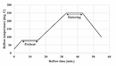 Figure 3. Sintering reflow profileThe solder balls used for the evaluation of SJR, were 0.6 mm diameter Sn-3.0Ag-0.5Cu (M705 / Senju metal). The reflow profile with a peak temperature of 260 degree C was applied for mounting the solder balls as shown in Figure 1. SJR was measured by ball pull (BP) test (4000 Plus / Nordson DAGE) as shown in Table 2.
The commercial product was used as the Ag sinter material. Figure 2 shows the Ag sintering joint reliability test method. First, the Ag sinter material is stretched by metal mask and printed by a squeegee onto the plated base material. The thickness of the Ag sinter material was adjusted to 150 μm by metal mask. Second, a plated Cu block with each deposit is put onto the printed Ag sinter material. After that, a little pressurization is vertically applied from the top of the plated Cu block. Finally, it is sintered by heating at 250 degree C for 10 minutes as shown in Figure 3. No pressurization is performed during sintering. Detailed Ag sintering joint reliability test conditions are shown in Table 4.
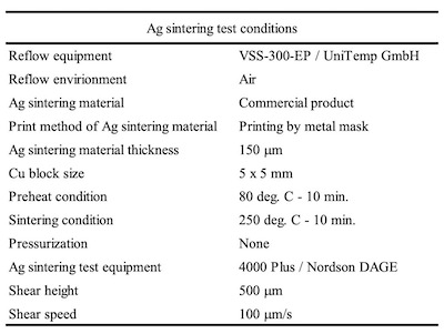 Table 4. Ag sintering test conditionsWBR of wedge bonding for Al wire was evaluated by wire bonder (HB16 / TPT) and pull test (DAGE SERIES 4000 / Nordson DAGE) as shown in Table 3.
The commercial product was used as the Ag sinter material. Figure 2 shows the Ag sintering joint reliability test method. First, the Ag sinter material is stretched by metal mask and printed by a squeegee onto the plated base material. The thickness of the Ag sinter material was adjusted to 150 μm by metal mask. Second, a plated Cu block with each deposit is put onto the printed Ag sinter material. After that, a little pressurization is vertically applied from the top of the plated Cu block. Finally, it is sintered by heating at 250 degree C for 10 minutes as shown in Figure 3. No pressurization is performed during sintering. Detailed Ag sintering joint reliability test conditions are shown in Table 4.
Results and Discussion
 Comparison of deposition rate between autocatalytic Ag bath and displacement Ag bath on Ni-P thickness 6 μm / Pd-P thickness 0.02 μmComparison of deposit performance between displacement Ag bath and autocatalytic Ag bath
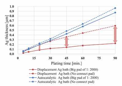
For the comparison of the deposition rate, the no connect pad and the big pad of 1: 2000 on the Uyemura test board A were measured. When using the displacement Ag bath, the thickness difference between the 2 different sized pads widened as the plating time increased. On the other hand, when using the autocatalytic Ag bath, the thickness increased linearly as prolonging the plating time regardless of the pad size.
The thickness distributions were compared by using 6 points on the Uyemura test board A: the no connect pad, the small pads of 1:1, 1:10, 1:100, 1:1000 and the big pad of 1: 2000. The target Ag thickness is 0.2 μm.
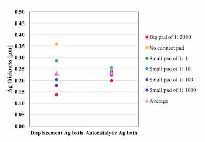 Figure 4. Comparison of thickness distribution between autocatalytic Ag bath and displacement Ag bath on Ni-P thickness 6 μm / Pd-P thickness 0.02 μmThe thickness distribution of the displacement Ag bath was 34.2 as a coefficient of variation (CV). On the other hand, because the autocatalytic reaction proceeds at all plated area simultaneously, the thickness distribution of the autocatalytic Ag bath was much smaller and the CV was 8.5 as shown in Figure 4.
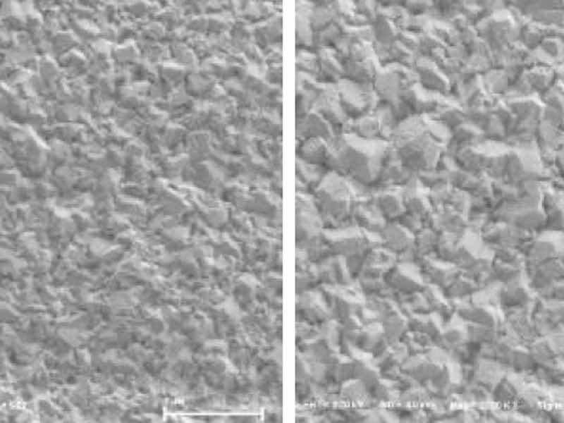
Surface images of ENEPIS and ENEPES deposit are shown in Figure 5, 6 for several Ag thickness. It seemed that the crystals of both the displacement Ag bath and the autocatalytic Ag bath became larger as the Ag thickness became thicker as shown in Figure 5, 6. Also if comparing to the deposits with Ag thicknesses of 0.5 μm, it seemed the surface roughness of Ag deposit with the displacement Ag bath looked slightly smoother than that of the autocatalytic Ag bath.
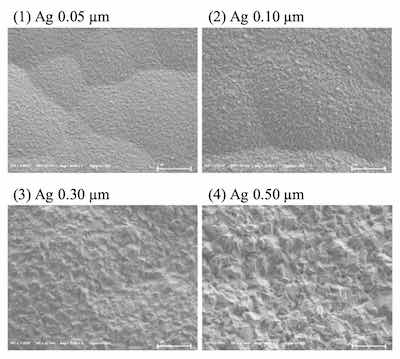 Figure 5. SEM images of ENEPIS deposit, Ni-P thickness; 6 μm, Pd-P thickness; 0.02 mm, Ag thickness; 0.05 μm, 0.10 μm, 0.30 μm and 0.5 μm, magnification; 20,000The grain sizes of both Ag deposits were investigated by EBSD analysis. Figure 7 shows the inverse pole figure (IPF) images for each metal (Ni, Pd, Ag), which shows crystal orientation (vertical plane) and the grain size. The average grain size of the Ag deposit with the autocatalytic Ag bath was 0.11 μm, which was slightly larger than that with the displacement Ag bath (0.08 μm). It seemed that these tendencies were relative to the results of the SEM observation, which the deposit from the displacement Ag bath looked smoother than that from the autocatalytic Ag bath.
The cross-section SEM images of ENEPIS and ENEPES were shown in Figure 8, 9 for several Ag thickness. The corrosion of Ni-P was observed when using the displacement Ag bath as shown in Figure 8. On the other hand, the corrosion of Ni-P was hardly observed when using the autocatalytic Ag bath as shown in Figure 9.
Solder joint reliability
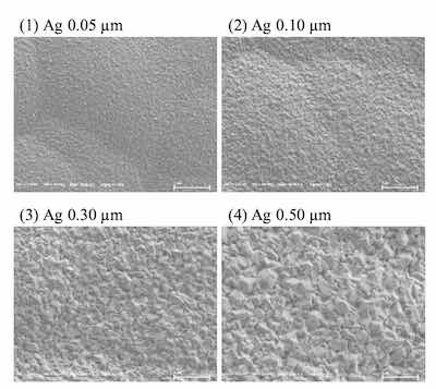 Figure 6. SEM images of ENEPES deposit, Ni-P thickness; 6 μm, Pd thickness; 0.02 μm, Ag thickness; 0.05 μm, 0.10 μm, 0.30 μm and 0.5 μm, magnification; 20,000For the evaluation of solder joint reliability (SJR) of the ENEPIS and ENEPES deposits after mounting the solder ball, BP test was evaluated by the failure mode after pulling the solder ball as shown in Figure 10. Failure modes were classified into 4 types, then scores were assigned to each type of failure mode. For the case of a complete break in the solder ball, a score of 5 was assigned (A mode). If the broken interface contained less than 25 % IMC, a score of 2.5 was assigned (B mode). Finally, if the broken interface contained more than 25 % IMC or voids, scores of zero were assigned (D, V mode). For instance, if all 20 balls were broken completely in the solder without IMC appearance, the total score would equal 100 since a score of 5 was assigned for each ball.
Solder balls of SAC305 were mounted by using a severe reflow profile of 260 degree C top to clarify the difference for each deposit. Total BP scores were shown in Table 5 for ENEPIG, ENEPIS and ENEPES deposit. When reflowed 3 times, BP scores were excellent in all conditions and there was no difference in each process. On the other hand, there was the difference in BP scores after 5 times reflow, depending on the reaction type of Ag bath. ENEPES had better SJR than ENEPIS. It is considered that the SJR has been affected by the occurrence of high quantities of Ni-P corrosion for ENEPIS. Also, ENEPES had equivalent SJR to ENEPIG.
Wire bonding reliability
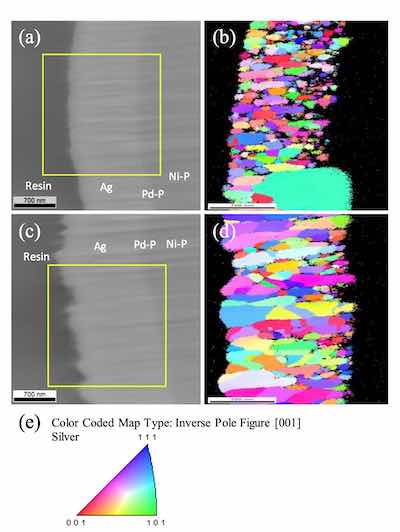 Figure 7. EBSD results; (a)cross section SEM image of ENEPIS, (b) IPF image of ENEPIS, (c)cross section SEM image of ENEPES, (d)IPF image of ENEPES, (e) Color coded map of IPF imagesWire bonding reliability (WBR) was evaluated by pull strengths of 1.0 mil-1% Si/Al wire pull testing for the samples shown in Table 6. All samples showed good pull strength that were more than 9 g and there was no difference in each process.
Ag sintering joint reliability
The Ag sintering joint reliability was evaluated by the shear strengths of 5 x 5 mm plated Cu block. The Ag sinter material, which was used in this report, has a maximum shear strength of approximately 35 MPa. The shear strength of ENEPIG was very low, approximately 13 MPa. On the other hand, the shear strengths of ENEPIS and ENEPES were relatively good, and the shear strength became stronger as the Ag thickness increased. When the Ag thickness was 0.3 μm and more, it was almost the same strength as the maximum shear strength of the Ag sinter material.
Conclusions
Several reliabilities of ENEPIS with a displacement reaction Ag bath and ENEPES with a autocatalytic reaction Ag bath were compared. ENEPES had better thickness distribution, and less Ni-P corrosion which resulted in better solder joint reliability. Both ENEPES and ENEPIS had good wire bonding reliability for Al wire. Also, when the Ag thickness of both ENEPES and ENEPIS was 0.3 μm and more, Ag sintering reliability could be satisfied. Thermal cycle testing after Ag sintering will be examined for ENEPIS and ENEPES as next steps.
Authors
Naoshi Nishimura, Mutsumi Komeyama, Tsuyoshi Maeda, Katsuhisa Tanabe and Shigeo Hashimoto C.Uyemura & Co., Ltd., Hirakata, Osaka, Japan; and Scott Larson, UIC Technical Center, Southington, Connecticut, USA
References
- Gourab Majumdar, Junji Yamada, "Latest Trend and Prospect of PowerModule Technology", MITSUBISHI DENKI GIHO - Vol.92 - No.3 - 2018
- Chen Chuantong, Suganuma Katsuaki, Engineering materials - Vol.70 - No.1 - Feb.2022
- T. Iwashige, K. Sugiura, T. Endo, K. Tsuruta, Y. Sakuma, S. Kurosaka, Y. Oda, C. Chen, S. Nagao, and K. Suganuma, " Metallization Technology of SiC Power Module in High Temperature Operation", 2018 International Conference on Electronics Packaging and iMAPS All Asia Conference (ICEPIAAC)
- Dai Ishikawa, Yuki Kawana, Chie Sugama, Hideo Nakako, Yoshinori Ejiri, Kazuhiko Kurafuchi, "Development of Pressure-less Sintering Copper Die- bonding Paste (I) ", MES2016
- Shouji Miura, Yasushi Ookura, Yoshifumi Okabe, Seiji Momota, "Development of Power Devices for Power Cards", DENSO technical review - Vol.16 - 2011
- Kunio Mano, Television - Vol.20 - No.6 - 1966
- Akira Chinda, Osamu Yoshioka, "Effect of Copper Strike Plating on Adhesion of Interface between Silver and Nickel Plating after Thermal Treatment", The Surface Finishing Society of Japan - Vol.45 No.1 - 1994
- R. Khabibullin, D. Ushakov, A. Afonenko, N. Shchavruk, D. Ponomarev, O. Volkov, V. Pavlovskiy, I. Vasil’evskii, D. Safonov, A. Dubinov, "Silver-based double metal waveguide for terahertz quantum cascade laser,", International Conference on Micro- and Nano-Electronics 2018 - Proc. of SPIE Vol.11022
- Kai Ojima, Jun Taniguch "Fabrication of nano metal grid pattern on the flexible substrate using a silver ink.", The Japan Society for Precision Engineering 2016 spring
- Tomomi Aoki, Jun-ishi Katayama, Kuniaki Otsuka, Hidemi Nawafune, "Optimization of Multilayer Surface Treatment System for LEDs Reflector", Journal of Japan Institute of Electronics Packaging - Vol.16 - No.6 - 2013
- Masato Ohmukai, Keiichi Ishida, Yasuo Tsutsumi, "Characteristics of DC Sputtering Apparatus and Deposition of Ag Thin Films", Memoirs of Akashi National College of Technology No.53 – Dec.2010
- Shigeo Hashimoto, Katsuhisa Tanabe, Masayuki Kiso, Daisuke Hashimoto, Don Gudeczauskas, "Study of the film characteristics with the neutral autocatalytic silver bath for LED-PKG finishing", SMTA International 2012