In this study, the Direct Immersion Gold (DIG) process is investigated.
 George Milad and Don GudeczauskasDIG is a process in which gold is plated directly on copper as a surface finish for printed circuit board and package applications. By examining the deposition reaction of the electroless flash gold plating bath, it was confirmed that, copper does not co-deposit with gold and also that the main driving force or deposition is an auto-catalytic reaction. In addition the effects of the copper surface roughness and deposition time on the deposit and solderability characteristics were examined. It was determined that copper surface roughness affects solder spread-ability, and that solder joint characteristics were excellent when the film thickness is within the range of 30 to 80 nm. Furthermore, good wire bonding characteristics were confirmed from deposits plated by a neutral pH, auto-catalytic type heavy electroless gold plating bath, atop the flash gold.
Introduction
Electronic components are normally mounted on to packages and printed circuit boards using solder. Lead free solder was investigated as an alternative solder material to tin/lead based material. Although many lead free solder compositions are available, the use of Sn/Ag/Cu solder materials are widely accepted in printed circuit board and package applications for its solder joint strength and reliability. Because the peak reflow temperature for Sn/Ag/Cu solder material ranges from 240 to 260°C and is higher than that of Sn/Pb eutectic solder, there is concern that surface mounting reliability will deteriorate. In this study, for printed circuit board and package surface finishing applications, Direct Immersion Gold (referred to as DIG), is introduced as a viable surface finish that is able to deposit a fine and uniform gold layer directly on the copper surfaces. The characteristics required for the success of the Direct Immersion Gold surface finish are as follows:
- Minimum corrosion of the copper surface during deposition (one of the causes of voiding after surface mounting).
- Gold plating layer has excellent coverage.
- Copper does not co-deposit with gold.
It was determined that it would be difficult to achieve feature 1) and feature 2) of the above mentioned characteristics by a displacement (immersion) gold deposition reaction. Therefore, an electroless gold plating bath that mainly deposits gold by an auto-catalytic reaction was developed.
Regarding feature 3) Copper co-deposition; theoretical evaluation was conducted by investigating the oxidation potential of the reducing agent contained in the DIG bath and the deposition potential of copper. Also, by conducting Auger analysis on the deposit, it was confirmed that copper does not contaminate the gold layer. Furthermore, by measuring the amount of dissolved copper and comparing it to the amount of deposited gold it was clear that the auto-catalytic reaction percentage is >80% of the total depositing reaction, as compared to the immersion reaction.
Gold coverage obtained by the DIG bath was examined by anodic electrical current measurement. By comparing a plating layer deposited by a displacement (immersion) type gold plating bath and plating layers deposited by the Direct Immersion Gold bath in various plating times, it was demonstrated that Direct Immersion Gold exhibits superior coverage as compared to standard immersion gold. Also, gold coverage on test coupons plated under 10 minutes differed significantly from those plated in excess of 10 minutes.
Test coupons for deposit characterization were plated for 20 minutes to give a gold layer thickness of approximately 50 nm. This was shown to give the optimum gold coverage as verified by SEM evaluation.
In order to study the relationship between copper surface roughness conditions and DIG gold deposit characteristics, solder joint reliability evaluations were conducted on substrates plated by Direct Immersion Gold with the copper surface micro-roughness adjusted by various copper etching conditions. Solder joint reliability was evaluated by examining solder ball spreading, ball shear testing, and inter-metallic (IMC) formation for both Sn/Pb eutectic solder and Sn/Ag/Cu solder.
Gold wire bonding is widely used as a mounting technique for IC chip applications. Test coupons for gold wire bonding characterization were prepared by plating 50 nm of DIG as above. In addition a 500 nm gold thickness test sample was also prepared by the deposition of an additional layer on top of the 50 nm of DIG. This new layer was deposited by a heavy deposition neutral pH, auto-catalytic electroless process.
Test Procedures and Results
 Confirmation of deposition reaction:
In order to determine the oxidation reaction of “DIG R”, which is the reducing agent of Direct Immersion Gold, the rest potential was measured using a gold electrode and a copper electrode. The standard electrode was Ag/AgCl, and the working electrode was copper and gold plate. Measuring temperature was 85°C.
Measuring solution:
- Solution A): DIG solution with no gold salts.
- Solution B): DIGsolution with no gold salts and no reducing agent “DIG R”
Test method and results are shown in Fig 1
From the results of this testing method, it should be noted that during the comparison of the solution with and without “DIG-R” (comparison of solution A and B), the rest potential of the gold electrode surface and copper electrode both fluctuate to a rest noble potential. This fluctuation in potential demonstrates the possibility that “DIG-R” is oxidizing at the gold electrode and copper electrode surface. Also, this potential was near equal at the copper electrode and gold electrode surface. This type of potential fluctuation demonstrates that it is difficult for a copper corrosion current to ocuur even if copper is immersed in the plating solution. If it is difficult for a copper corrosion current to generate during plating, then the copper dissolution amount according to the plating reaction is reduced. Also, because the oxidation reaction of the reducing agent is nearly equal to the rest potential of copper, it is easily seen that it is difficult for copper to deposit with the gold.
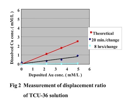 Moreover, by conducting a plating test using a 10 L test cell and measuring the gold deposition amount and the amount of copper dissolution into the plating solution, it was determined that the main deposition reaction is an auto-catalytic reaction. The Direct Immersion Gold bath was adjusted during plating by analyzing the gold concentration amount with atomic absorption spectrometry, and gold cyanide and “DIG-R” were replenished according to the gold consumption amount. Copper clad laminate boards (FR-4) were used as test substrate printed circuit boards. Bath load factor was 2dm2/L, and test substrate boards were changed by two methods, every twenty minutes and every 8 hours. The relationship between the gold deposition amount and copper dissolution concentrationin the plating solution is shown in Fig. 2.
From this result, it was confirmed that the dissloved copper concentration in Direct Immersion Gold solution is lower compared to the copper dissolution concentration that can be theoretically calculated assuming the plating bath deposition reaction is 100% displacement (immersion) reaction. It was also confirmed that the copper dissolution amount differs according to the exchanging cycle times of the test printed circuit boards. From these results, we assume that the main reaction for DIG bath is an auto-catalytic reaction. This result confirm the rest potential measurement.
 Also, by conducting Auger qualitative analysis of gold film deposited on test coupons that were plated with plating baths containing 50mg/L of copper, results showed that copper does not co-deposit within the gold.
The standard DIG plating process utilized to evaluate the gold deposit is shown in table 1.
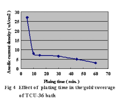
In order to confirm the optimum plating time, the relationship between gold coverage and plating time were investigated by anodic electric current measurement. This method to measure gold coverage is performed by using 5% sodium sulfate with 0.1% tartaric acid as the electrolyte, and measuring the anodic current density when a electric potential of 70mV is applied to the Ag/AgCl reference electrode. Test substrates were prepared by applying electrolytic acid copper plating (20um) to copper clad laminate boards and adjusting the surface area to 1 cm X 1 cm dimensions with masking tape. Measurement results of the relationship between DIG plating time and anodic current density are shown in Fig.4. The comparison with a conventional 100% displacement (immersion) reaction electroless gold plating bath is shown in Fig.5. Also, the relationship between Direct Immersion Gold plating time and gold plating layer thickness is shown in Fig.6.
Table 1 Standard DIG Process
| Cleaner | ACL-009 | 50°C. | 5 Min. Rinse |
| Acid Rinse | 10% Sulfuric Acid. | 25°C | 1 Min. Rinse |
| Soft Etching | 25°C | 2 Min. Rinse | |
| Acid Rinse | 10% Sulfuric Acid | 25°C | 1 Min. Rinse |
| Immersion Rinse | TCU-36 | 80°C | 20 Min. Rinse |
In the anodic eletrolysis conditions used in this evaluation, gold does not dissolve and only copper dissolves.
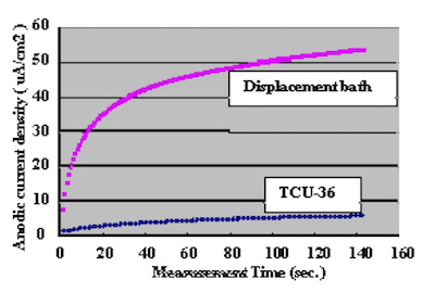 Figure 5Therefore we understand it is possible to compare the gold surface coverage ratio by measuring the anodic current density. The results in Fig.4 demonstrate that the surface coverage ratio does not increase much after the first ten minutes of plating. In this study, the plating time was adjusted so that it was possible to deposit a gold plating layer of 50 nm (20 minutes) on the test substrates.
The surface SEM photographs of variable plating time coupons are shown in Fig. 7. Because the gold plating layer thickness deposited by Direct Immersion Gold is 50 nm, copper surface roughness has a great influence on gold coverage characteristics. In order to investigate the relationship between copper surface roughness and gold plating layer characteristics, test cuopons with relatively severe buff polishing after electrolytic acid copper plating were prepared. Solder mask was applied to the test cuopons, and by using a special copper etching agent CZ (Mec Company Ltd.) process, test coupons of different surface roughness were made by adjusting the CZ copper etching amounts to 0, 1, 2, and 3um. An SPS (sodium persulfate) bath and a sulfuric acid/hydrogen peroxide bath were utilized as a soft etching process before plating with DIG in order to adjust surface roughness. By using test coupons with different copper surface roughness and different soft etching conditions in the pre plating process, the influence copper surface roughness has on solder joint characteristics was confirmed. The relation between each soft etching condition and surface roughness is shown in Fig.8. A laser microscope (KEYENCE Corporation VK-8550) was utilized for surface roughness measurement.
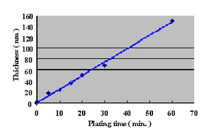 Figure 6As a result, a smoother (more even) copper surface was obtained by a sulfuric acid/hydrogen peroxide type etching bath compaired to a sodium persulfate etching bath.
Direct Immersion Gold was deposited for 20 minutes to the copper surface roughness test substrates shown in Fig. 8. Solder spreading ratio was evaluated using these test cuopons. The test results are shown in Fig.9. Also, solder spreading ratio comparison between eutectic Pb/Sn solder and lead free solder are shown in Fig.10.
Solder Spread Ratio Measurement
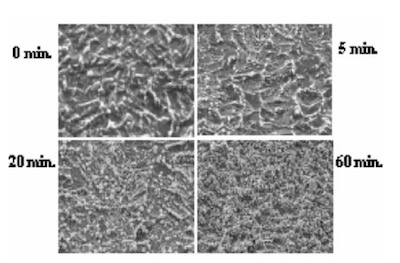 Figure 7The test method for solder spread ratio measurement was as follows:
R type flux (Alpha metal Co. R5003, R Type) was applied on the test coupon and solder balls (Pb/Sn eutectic and Sn/4.0%Ag/0.5%Cu) of 0.75 mm in diameter were placed on the coupon which was then placed on a hot plate (230 oC for Pb/Sn eutectic solder, 260°C for lead free solder) for 40 seconds. At the respective temperature the solder ball would melt down and spread out on the coupon. The solder spreading ratio was then calculated as follows:
Solder spreading ratio = (Solder spreading area) / (Original solder ball volume)
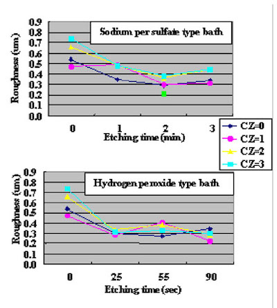 Figure 8The results indicate that the solder spreading ratio was larger when the copper surface was rougher. Also, lead free solder results were inferior (spread less) as compared to Pb/Sn eutectic solder. It is necessary to understand this characteristic when lead free solder is utilized.
Solder ball shear testing procedure was as follows. After the DIG finish was applied to the test substrate, Pb/Sn eutectic and Sn/Ag/Cu solder balls of 0.75 mm in diameter were soldered to 0.6 mm pads in diameter. Evaluation conditions are shown in Table 2 and test results are shown in Fig.11.
Table 2 Solder Ball Shear Conditions
- Sn/Pb: 63/37 Senjyukinzoku, SaprkballS, 0.76mm
- Sn/Ag/Cu: 95.5/4.0/0.5 Senjyukinzoku, Eco-solderball S, 0.76mm
Reflow Conditions
- Sn/Pb solder: 230°C, 40 sec, hot plate in air
- Sn/Ag/Cu: 260°C, 40 sec, hot plate in air
- Flux: Alphametal R5003 (Rtype)
Equipment and Test Conditions
- Dage#4000
- Shear Speed: 4,000 μm/sec
- Tool height: 50 μm
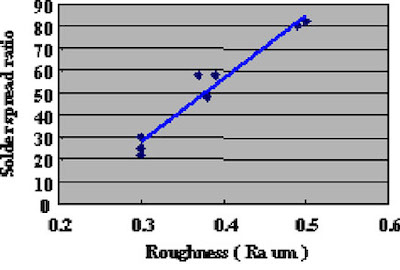 Figure 9In the case of Pb/Sn eutectic solder, a significant difference in ball shear test results could not be confirmed. On the other hand, Sn/Ag/Cu solder results showed that copper surface etching methods had a direct effect on voids in the solder, and therefore indicate that it is necessary for an optimum etching method to be chosen.
It is concluded, that the higher reflow temperature was a reason why the solder spreading ratio results for Sn/Ag/Cu solder were inferior. It may be necessary for future testing to actaully pull an IC chip after it has been mounted.
Furthermore, in order to confirm long term joint reliability after mounting, shear testing and IMC cross section observation were conducted on test cuopons that were heat treated at 150°C for 1,000 hours.
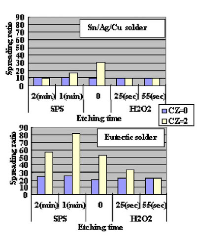 Figure 10In order to confirm the wire bonding characteristics of DIG finishing, test coupons with gold thickness of 50 nm (Flash gold only) and 500 nm (Flash and heavy gold) were prepared (standard plating process is shown in Table 3).
Two types of 50 nm gold thickness test substrates were prepared, one without heat treatment and one with heat treatment at 155°C for 3 hours. Also, the 500 nm test coupons were heat treated per in-house pre-wire bonding procedure (heat treatment at 175°C for 3, 6, 10 and 16 hours), and wire bonding characteristics were evaluated. The wire bonding conditions are shown in Table 4.
It is known that bonding strength will decrease or bonding would fail, if there are oxidized metals on the gold surface. Good wire bonding results were obtained from flash gold test coupons (Direct Immersion Gold finishing) that were not heat treated. This reconfirmed that the Direct Immersion Gold film was high in purity and had excellent gold coverage.
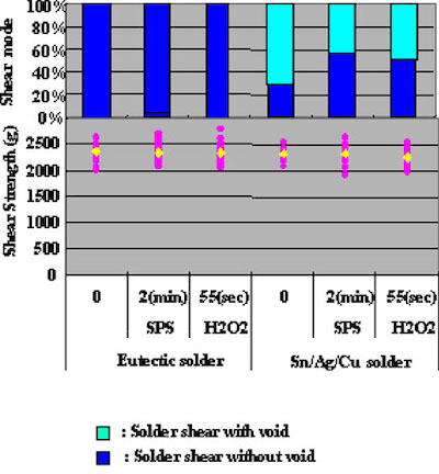 Figure 11Table 4 Wire Bonding Conditions
- Model: KS 4524A Semi-auto
- Wire size” 25μm
- Capillary part #: 4047220010-320
- Frequency US: 60Hz
- 1st Bond
- 2nd Bond
- Power: 130 mW; 190mW
- Time: 10msec; 15msec
- Force: 30g; 90g
Although the wire bonding evaluation results after heat conditioning of thicker gold films (falsh and heavy dep) were inferior compared to the conventional test coupons that include a Ni-P layers, it was demonstrated that it is possible to wire bond on heavy gold films which have been deposited directly on copper.
Conclusion
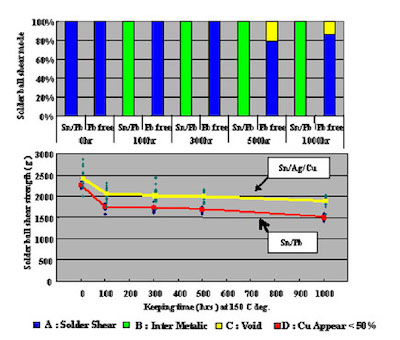 Figure 12Many processes are being proposed as a final finishes for printed circuit board and package applications. In this study, a finishing process that can directly deposit gold onto the copper surface by utilizing an electroless plating process has been presented. It was confirmed that it is possible to directly deposit gold on the copper surface with excellent coverage and without creating defects on the copper surface, because the main gold depositing reaction is an auto-catalytic and not a displacement one. Furthermore, by combining a neutral auto-catalytic heavy gold electroless plating bath, a heavy gold layer was deposited directly on the copper surface. The applicability of solder mounting and gold wire bonding on these gold plating layers (flash 50 nm and heavy 500 nm) directly on copper was demonstrated.
Authors: George Milad and Don Gudaczauskas; Uyemura International Corporation; and Shigeo Hashimoto, Masayuki Kiso, Yukinori Oda, Horshi Otake C.Uyemura & Co., Ltd. Central Research Laboratory, Osaka Japan.
Visit www.Uyemura.com